

S-1009N17I-I4T1U
Basic Information Overview
- Category: Integrated Circuit (IC)
- Use: Power Management
- Characteristics: Low Dropout Voltage Regulator
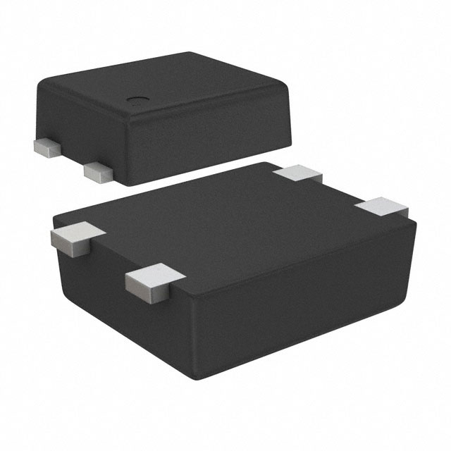
- Package: SOT-23-5
- Essence: Voltage Regulator IC
- Packaging/Quantity: Tape and Reel, 3000 pieces per reel
Specifications
- Input Voltage Range: 2.5V to 6.0V
- Output Voltage Range: 1.2V to 5.5V
- Maximum Output Current: 100mA
- Dropout Voltage: 160mV @ 100mA
- Quiescent Current: 30µA (typical)
- Operating Temperature Range: -40°C to +85°C
Detailed Pin Configuration
The S-1009N17I-I4T1U IC has a total of five pins arranged in the following configuration: 1. VIN: Input voltage pin 2. GND: Ground pin 3. EN: Enable pin 4. VOUT: Output voltage pin 5. NC: No connection pin
Functional Features
- Low dropout voltage for efficient power management
- Wide input voltage range allows flexibility in power supply design
- Low quiescent current for power-saving applications
- Built-in overcurrent protection for enhanced reliability
- Thermal shutdown protection prevents IC damage due to excessive heat
Advantages
- Compact SOT-23-5 package enables space-saving designs
- Wide input voltage range accommodates various power sources
- Low dropout voltage ensures stable output even with low input voltages
- Low quiescent current minimizes power consumption
- Overcurrent and thermal shutdown protection enhance system reliability
Disadvantages
- Limited maximum output current may not be suitable for high-power applications
- Restricted operating temperature range may limit usage in extreme environments
Working Principles
The S-1009N17I-I4T1U is a low dropout voltage regulator IC that regulates the output voltage based on the input voltage. It operates by comparing the reference voltage with the feedback voltage and adjusts the pass transistor accordingly to maintain a stable output voltage. The enable pin allows for easy control of the IC's operation.
Detailed Application Field Plans
The S-1009N17I-I4T1U IC finds applications in various fields, including but not limited to: 1. Battery-powered devices: Portable electronics, wireless sensors, and wearables. 2. Automotive electronics: Infotainment systems, dashboard displays, and lighting controls. 3. Industrial equipment: Sensor modules, motor control circuits, and power supply units. 4. Communication devices: Mobile phones, tablets, and routers. 5. Consumer electronics: Digital cameras, audio players, and gaming consoles.
Detailed and Complete Alternative Models
- S-1009N17I-I4T1G: Similar specifications and features, available in a different package (SOT-89-5).
- S-1009N17I-I4T1R: Improved version with lower dropout voltage and higher maximum output current.
- S-1009N17I-I4T1V: Adjustable output voltage version with a wider range of output voltage options.
- S-1009N17I-I4T1P: Package variant with enhanced thermal dissipation capabilities.
(Note: These alternative models are provided as examples and may not be an exhaustive list.)
This entry provides comprehensive information about the S-1009N17I-I4T1U voltage regulator IC. Its basic information, specifications, pin configuration, functional features, advantages, disadvantages, working principles, application field plans, and alternative models are covered.
قم بإدراج 10 أسئلة وإجابات شائعة تتعلق بتطبيق S-1009N17I-I4T1U في الحلول التقنية
Sure! Here are 10 common questions and answers related to the application of S-1009N17I-I4T1U in technical solutions:
Q1: What is S-1009N17I-I4T1U? A1: S-1009N17I-I4T1U is a specific model or part number of a component used in technical solutions, such as electronic circuits or systems.
Q2: What is the purpose of S-1009N17I-I4T1U? A2: The purpose of S-1009N17I-I4T1U is to perform a specific function within a technical solution, which could include voltage regulation, power management, or signal conditioning.
Q3: How does S-1009N17I-I4T1U work? A3: S-1009N17I-I4T1U works by receiving an input signal or voltage and providing a regulated output signal or voltage based on its internal circuitry and design.
Q4: What are the key features of S-1009N17I-I4T1U? A4: Some key features of S-1009N17I-I4T1U may include high efficiency, low power consumption, small form factor, wide input voltage range, and overcurrent/overvoltage protection.
Q5: In what applications can S-1009N17I-I4T1U be used? A5: S-1009N17I-I4T1U can be used in various applications, including but not limited to consumer electronics, industrial automation, telecommunications, automotive systems, and medical devices.
Q6: What is the maximum input voltage supported by S-1009N17I-I4T1U? A6: The maximum input voltage supported by S-1009N17I-I4T1U is typically specified in the datasheet provided by the manufacturer. It is important to refer to the datasheet for accurate information.
Q7: Can S-1009N17I-I4T1U handle high current loads? A7: Yes, S-1009N17I-I4T1U is designed to handle a certain range of current loads. The maximum current handling capability is usually specified in the datasheet.
Q8: Is S-1009N17I-I4T1U compatible with other components or systems? A8: S-1009N17I-I4T1U is designed to be compatible with various components and systems that operate within its specified voltage and current ranges. However, it is always recommended to verify compatibility before integration.
Q9: Are there any specific precautions to consider when using S-1009N17I-I4T1U? A9: Precautions may include proper heat dissipation, input/output voltage limitations, adherence to manufacturer's guidelines, and protection against ESD (electrostatic discharge).
Q10: Where can I find more information about S-1009N17I-I4T1U? A10: More detailed information about S-1009N17I-I4T1U can be found in the product datasheet provided by the manufacturer. Additionally, online resources, forums, or contacting the manufacturer directly can provide further information and support.