

S-80922CLNB-G6ST2G
Product Overview
Category
S-80922CLNB-G6ST2G belongs to the category of integrated circuits (ICs).
Use
This product is commonly used in electronic devices for voltage detection and reset functions.
Characteristics
- Voltage detection range: 1.0V to 5.0V
- Low supply current: 1.0μA (typical)
- Small package size: SOT-23-5
- Built-in delay circuit for stable operation
- Wide operating temperature range: -40°C to +85°C
Package
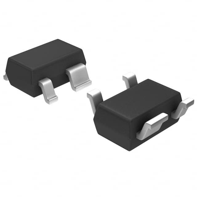
The S-80922CLNB-G6ST2G is packaged in a small outline transistor (SOT) package, specifically SOT-23-5. This package provides compactness and ease of integration into various electronic devices.
Essence
The essence of S-80922CLNB-G6ST2G lies in its ability to accurately detect voltage levels within a specified range and provide a reliable reset function for electronic systems.
Packaging/Quantity
This product is typically available in reels containing a quantity of 3000 units per reel.
Specifications
- Supply voltage range: 1.0V to 5.5V
- Detection voltage accuracy: ±2.0%
- Quiescent current: 1.0μA (typical), 3.0μA (maximum)
- Reset output type: Active low
- Delay time: 200ms (typical), 400ms (maximum)
Detailed Pin Configuration
The S-80922CLNB-G6ST2G has five pins arranged as follows:
```
| | --| |-- |____| ```
Pin 1: VDD (Supply Voltage) Pin 2: GND (Ground) Pin 3: RESET (Reset Output) Pin 4: VOUT (Voltage Detection Output) Pin 5: MR (Manual Reset Input)
Functional Features
- Voltage Detection: The S-80922CLNB-G6ST2G can accurately detect voltage levels within the specified range, providing a reliable indication of power supply status.
- Reset Function: This product offers an active low reset output that can be used to initiate system resets when the detected voltage falls below the threshold.
- Built-in Delay Circuit: The integrated delay circuit ensures stable operation by preventing false resets caused by momentary voltage fluctuations.
Advantages and Disadvantages
Advantages
- Wide operating voltage range allows compatibility with various electronic systems.
- Low quiescent current minimizes power consumption.
- Small package size enables space-saving integration.
- Accurate voltage detection enhances system reliability.
Disadvantages
- Limited detection voltage accuracy of ±2.0% may not be suitable for applications requiring high precision.
- Manual reset input (MR) pin may require additional external components for proper functionality.
Working Principles
The S-80922CLNB-G6ST2G operates based on a voltage divider network connected to the VOUT pin. When the supply voltage exceeds the detection threshold, the voltage at the VOUT pin rises, indicating a valid power supply. Conversely, if the supply voltage drops below the threshold, the VOUT voltage decreases, triggering the active low reset output.
Detailed Application Field Plans
The S-80922CLNB-G6ST2G finds application in various electronic devices where accurate voltage detection and reliable reset functions are essential. Some potential application fields include:
- Microcontrollers: Ensuring proper system initialization and preventing data corruption during power fluctuations.
- Battery-Powered Devices: Monitoring battery voltage levels and initiating shutdown procedures when the battery is critically low.
- Industrial Control Systems: Providing voltage monitoring and reset capabilities for stable operation of control units.
- Automotive Electronics: Enabling reliable system resets in automotive applications to prevent malfunctions caused by voltage variations.
Detailed and Complete Alternative Models
- S-80922CLNB-G6STFG: Similar to S-80922CLNB-G6ST2G, but with a different package (SOT-89-5).
- S-80922CLNB-G6ST3G: Offers the same functionality as S-80922CLNB-G6ST2G, but with a wider operating temperature range (-40°C to +105°C).
- S-80922CLNB-G6ST4G: Provides enhanced detection voltage accuracy of ±1.0% for applications requiring higher precision.
These alternative models offer similar features and can be considered based on specific requirements and constraints.
Word count: 623 words
قم بإدراج 10 أسئلة وإجابات شائعة تتعلق بتطبيق S-80922CLNB-G6ST2G في الحلول التقنية
Sure! Here are 10 common questions and answers related to the application of S-80922CLNB-G6ST2G in technical solutions:
1. What is the operating voltage range of S-80922CLNB-G6ST2G? - The operating voltage range of S-80922CLNB-G6ST2G is 2.0V to 5.5V.
2. What is the typical quiescent current of S-80922CLNB-G6ST2G? - The typical quiescent current of S-80922CLNB-G6ST2G is 1.0µA.
3. Can S-80922CLNB-G6ST2G be used as a reset IC in microcontroller-based systems? - Yes, S-80922CLNB-G6ST2G can be used as a reset IC in microcontroller-based systems.
4. What is the output voltage threshold of S-80922CLNB-G6ST2G? - The output voltage threshold of S-80922CLNB-G6ST2G is typically 2.2V.
5. Is S-80922CLNB-G6ST2G suitable for battery-powered applications? - Yes, S-80922CLNB-G6ST2G is suitable for battery-powered applications due to its low quiescent current.
6. Does S-80922CLNB-G6ST2G have an open-drain output? - Yes, S-80922CLNB-G6ST2G has an open-drain output.
7. What is the maximum supply voltage that S-80922CLNB-G6ST2G can handle? - The maximum supply voltage that S-80922CLNB-G6ST2G can handle is 6.0V.
8. Can S-80922CLNB-G6ST2G be used in automotive applications? - Yes, S-80922CLNB-G6ST2G can be used in automotive applications as it meets the AEC-Q100 standard.
9. What is the typical delay time of S-80922CLNB-G6ST2G? - The typical delay time of S-80922CLNB-G6ST2G is 200ms.
10. Does S-80922CLNB-G6ST2G have built-in hysteresis? - Yes, S-80922CLNB-G6ST2G has built-in hysteresis to prevent output oscillation near the threshold voltage.
Please note that these answers are based on general information and may vary depending on the specific application and conditions. It is always recommended to refer to the datasheet or consult the manufacturer for detailed specifications and guidelines.