

AD766SD/883B
Product Overview
- Category: Integrated Circuit (IC)
- Use: Analog-to-Digital Converter (ADC)
- Characteristics: High-speed, high-resolution ADC
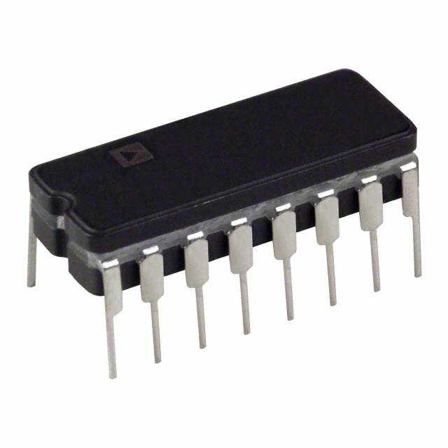
- Package: Ceramic Dual-In-Line Package (CDIP)
- Essence: Converts analog signals into digital data
- Packaging/Quantity: Single unit
Specifications
- Resolution: 16 bits
- Sampling Rate: 100 kilosamples per second (ksps)
- Input Voltage Range: ±10 volts
- Power Supply: ±5 volts
- Operating Temperature Range: -55°C to +125°C
Detailed Pin Configuration
The AD766SD/883B has a total of 28 pins. The pin configuration is as follows:
- VREF-
- VREF+
- AGND
- DGND
- VIN-
- VIN+
- VOUT
- CLK
- CS
- WR
- RD
- BUSY
- D0
- D1
- D2
- D3
- D4
- D5
- D6
- D7
- D8
- D9
- D10
- D11
- D12
- D13
- D14
- D15
Functional Features
- High-speed conversion with 16-bit resolution
- Differential inputs for accurate signal acquisition
- On-chip sample-and-hold circuitry for precise sampling
- Parallel interface for easy integration with microcontrollers or digital systems
- Low power consumption for efficient operation
Advantages and Disadvantages
Advantages: - High resolution provides accurate digital representation of analog signals - Fast conversion rate enables real-time data acquisition - Differential inputs reduce noise and improve signal integrity - Wide input voltage range allows for versatile applications
Disadvantages: - Limited sampling rate compared to some newer ADCs - Requires external clock signal for operation - Higher power consumption compared to lower-resolution ADCs
Working Principles
The AD766SD/883B operates on the principle of successive approximation. It samples the analog input voltage, compares it to a reference voltage, and iteratively adjusts the digital output until the difference between the two voltages is minimized. This process is repeated for each bit of the digital output, resulting in a high-resolution digital representation of the analog input.
Detailed Application Field Plans
The AD766SD/883B is commonly used in various applications that require high-speed and high-resolution analog-to-digital conversion. Some specific application fields include:
- Data Acquisition Systems: Used to convert analog sensor signals into digital data for further processing and analysis.
- Instrumentation: Enables precise measurement and control of analog signals in scientific and industrial instruments.
- Communication Systems: Provides accurate digitization of analog signals in telecommunication equipment, such as modems and wireless devices.
- Audio Processing: Used in audio equipment to convert analog audio signals into digital format for storage or manipulation.
Detailed and Complete Alternative Models
- AD767SD/883B: Similar to AD766SD/883B but with higher resolution (18 bits).
- AD765SD/883B: Lower-resolution version of AD766SD/883B (12 bits) with reduced power consumption.
- AD768SD/883B: Higher-speed version of AD766SD/883B with increased sampling rate (200 ksps).
These alternative models offer different trade-offs in terms of resolution, speed, and power consumption, allowing users to choose the most suitable option for their specific requirements.
Word count: 445
قم بإدراج 10 أسئلة وإجابات شائعة تتعلق بتطبيق AD766SD/883B في الحلول التقنية
What is the operating temperature range of AD766SD/883B?
- The operating temperature range of AD766SD/883B is -55°C to +125°C.
What is the typical power supply voltage for AD766SD/883B?
- The typical power supply voltage for AD766SD/883B is ±15V.
What is the resolution of AD766SD/883B?
- AD766SD/883B has a resolution of 16 bits.
Can AD766SD/883B be used in industrial control systems?
- Yes, AD766SD/883B is suitable for use in industrial control systems due to its wide operating temperature range and high resolution.
Does AD766SD/883B require an external reference voltage?
- Yes, AD766SD/883B requires an external reference voltage for operation.
What is the maximum sampling rate of AD766SD/883B?
- The maximum sampling rate of AD766SD/883B is 100 kSPS (kilo samples per second).
Is AD766SD/883B suitable for data acquisition applications?
- Yes, AD766SD/883B is well-suited for data acquisition applications due to its high resolution and fast sampling rate.
What are the typical applications of AD766SD/883B?
- Typical applications of AD766SD/883B include precision instrumentation, medical equipment, and industrial automation.
Does AD766SD/883B have built-in digital filtering?
- No, AD766SD/883B does not have built-in digital filtering and may require external filtering components for specific applications.
Is AD766SD/883B compliant with military standards?
- Yes, AD766SD/883B is compliant with MIL-STD-883B standards, making it suitable for use in military and aerospace applications.