

ADCMP552BRQ
Product Overview
Category
ADCMP552BRQ belongs to the category of analog-to-digital converters (ADCs).
Use
This product is primarily used for converting analog signals into digital format.
Characteristics
- High precision conversion
- Low power consumption
- Wide input voltage range
- Fast conversion speed
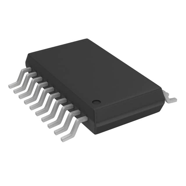
Package
ADCMP552BRQ comes in a compact and durable package, ensuring protection during transportation and handling.
Essence
The essence of ADCMP552BRQ lies in its ability to accurately convert analog signals into digital data, enabling further processing and analysis.
Packaging/Quantity
Each package of ADCMP552BRQ contains one unit of the converter.
Specifications
- Resolution: 12 bits
- Input Voltage Range: 0V to 5V
- Conversion Speed: 1 MSPS (Mega Samples Per Second)
- Power Supply: 3.3V
- Operating Temperature Range: -40°C to +85°C
Detailed Pin Configuration
- VDD: Power supply pin
- VREF: Reference voltage input
- VIN: Analog input voltage
- GND: Ground pin
- CLK: Clock input
- DOUT: Digital output
- CS: Chip select input
- SCLK: Serial clock input
Functional Features
- High-resolution conversion for accurate signal representation
- Fast conversion speed enables real-time data acquisition
- Low power consumption for energy-efficient operation
- Wide input voltage range allows compatibility with various signal sources
- Easy integration with microcontrollers and other digital systems
Advantages
- Precise and reliable conversion results
- Compact size for space-constrained applications
- Low power consumption extends battery life
- Versatile input voltage range accommodates diverse signal sources
- Compatibility with various digital systems enhances flexibility
Disadvantages
- Limited resolution compared to higher-end ADCs
- Relatively slower conversion speed compared to some competitors
- Requires external clock source for operation
Working Principles
ADCMP552BRQ operates on the principle of successive approximation. It samples the analog input voltage and compares it with a reference voltage. By iteratively adjusting the digital output, it converges towards an accurate representation of the analog signal.
Detailed Application Field Plans
ADCMP552BRQ finds applications in various fields, including: 1. Industrial automation: for monitoring and control systems 2. Medical devices: for precise measurement and analysis 3. Communication systems: for signal processing and modulation 4. Automotive electronics: for sensor data acquisition 5. Consumer electronics: for audio and video signal processing
Detailed and Complete Alternative Models
- ADCMP551BRQ: Similar specifications but with 10-bit resolution
- ADCMP553BRQ: Higher resolution (14 bits) with slightly slower conversion speed
- ADCMP554BRQ: Higher resolution (16 bits) with similar conversion speed
These alternative models offer different trade-offs in terms of resolution and conversion speed, allowing users to choose according to their specific requirements.
Word count: 511 words
قم بإدراج 10 أسئلة وإجابات شائعة تتعلق بتطبيق ADCMP552BRQ في الحلول التقنية
Sure! Here are 10 common questions and answers related to the application of ADCMP552BRQ in technical solutions:
Question: What is ADCMP552BRQ?
- Answer: ADCMP552BRQ is a high-speed comparator integrated circuit (IC) that can be used in various technical solutions.Question: What is the operating voltage range of ADCMP552BRQ?
- Answer: The operating voltage range of ADCMP552BRQ is typically between 2.7V and 5.5V.Question: What is the maximum input voltage range of ADCMP552BRQ?
- Answer: The maximum input voltage range of ADCMP552BRQ is typically between GND and VCC.Question: What is the output type of ADCMP552BRQ?
- Answer: ADCMP552BRQ has an open-drain output type, which means it can sink current but cannot source current.Question: What is the typical response time of ADCMP552BRQ?
- Answer: The typical response time of ADCMP552BRQ is around 8 ns.Question: Can ADCMP552BRQ operate in both single-ended and differential mode?
- Answer: Yes, ADCMP552BRQ can operate in both single-ended and differential mode, depending on the application requirements.Question: What is the input offset voltage of ADCMP552BRQ?
- Answer: The input offset voltage of ADCMP552BRQ is typically very low, around a few millivolts.Question: Does ADCMP552BRQ have built-in hysteresis?
- Answer: Yes, ADCMP552BRQ has built-in hysteresis, which helps to prevent oscillations and improve noise immunity.Question: Can ADCMP552BRQ be used in high-frequency applications?
- Answer: Yes, ADCMP552BRQ is designed for high-speed operation and can be used in high-frequency applications.Question: What is the package type of ADCMP552BRQ?
- Answer: ADCMP552BRQ is available in a small outline integrated circuit (SOIC) package.
Please note that the answers provided here are general and may vary depending on the specific datasheet and application requirements.