

ADCMP572BCPZ-WP
Product Overview
Category
ADCMP572BCPZ-WP belongs to the category of analog-to-digital converters (ADCs).
Use
This product is primarily used for converting analog signals into digital data.
Characteristics
- High precision and accuracy
- Fast conversion speed
- Low power consumption
- Wide input voltage range
- Compact package size
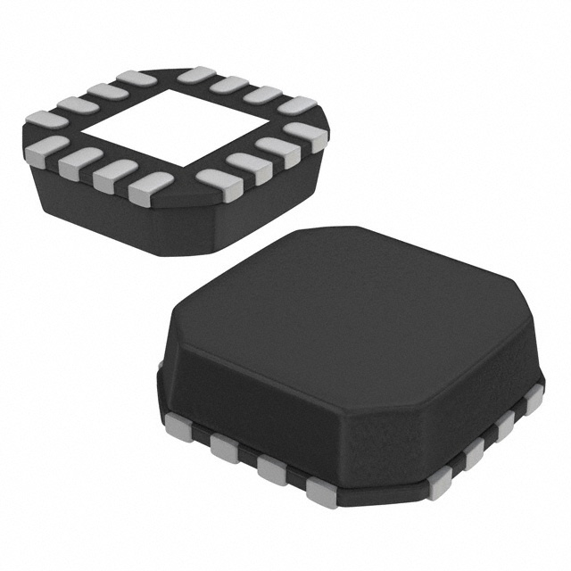
Package
ADCMP572BCPZ-WP is available in a small form factor package, which ensures easy integration into various electronic systems.
Essence
The essence of ADCMP572BCPZ-WP lies in its ability to accurately convert analog signals into digital format, enabling further processing and analysis.
Packaging/Quantity
This product is typically packaged in reels or trays, with a quantity of 250 units per reel/tray.
Specifications
- Resolution: 12 bits
- Sampling Rate: 1 MSPS (Million Samples Per Second)
- Input Voltage Range: 0V to Vref
- Power Supply: 2.7V to 5.5V
- Operating Temperature Range: -40°C to +85°C
- Interface: Serial Peripheral Interface (SPI)
Detailed Pin Configuration
- VDD: Power supply voltage
- VREF: Reference voltage for ADC conversion
- VIN: Analog input voltage
- GND: Ground reference
- SCLK: Serial clock input for SPI communication
- DIN: Serial data input for SPI communication
- DOUT: Serial data output for SPI communication
- CS: Chip select input for SPI communication
Functional Features
- High-resolution conversion
- Low noise and distortion
- Programmable gain amplifier
- Internal voltage reference
- Flexible power supply options
- Easy interfacing with microcontrollers and digital systems
Advantages and Disadvantages
Advantages
- High precision and accuracy in analog-to-digital conversion
- Fast conversion speed enables real-time data acquisition
- Low power consumption for energy-efficient applications
- Wide input voltage range allows compatibility with various signal sources
- Compact package size facilitates integration into space-constrained designs
Disadvantages
- Limited resolution compared to higher-end ADCs
- Relatively higher cost compared to lower-resolution alternatives
- Requires external voltage reference for optimal performance
Working Principles
ADCMP572BCPZ-WP utilizes the successive approximation register (SAR) architecture for analog-to-digital conversion. It samples the analog input voltage, compares it with a reference voltage, and generates a digital output representing the input voltage value.
Detailed Application Field Plans
ADCMP572BCPZ-WP finds applications in various fields, including: 1. Industrial automation 2. Medical instrumentation 3. Communication systems 4. Test and measurement equipment 5. Automotive electronics
Detailed and Complete Alternative Models
- ADCMP573BCPZ-WP: 14-bit resolution ADC with similar features and package.
- ADCMP571BCPZ-WP: 10-bit resolution ADC with similar features and package.
- ADCMP574BCPZ-WP: 16-bit resolution ADC with similar features and package.
(Note: The above alternative models are from the same product family and share common characteristics with ADCMP572BCPZ-WP.)
Word count: 389 words
قم بإدراج 10 أسئلة وإجابات شائعة تتعلق بتطبيق ADCMP572BCPZ-WP في الحلول التقنية
Sure! Here are 10 common questions and answers related to the application of ADCMP572BCPZ-WP in technical solutions:
Q: What is the ADCMP572BCPZ-WP? A: The ADCMP572BCPZ-WP is a high-speed comparator designed for use in various technical applications.
Q: What is the operating voltage range of the ADCMP572BCPZ-WP? A: The ADCMP572BCPZ-WP operates within a voltage range of 2.7V to 5.5V.
Q: What is the typical response time of the ADCMP572BCPZ-WP? A: The typical response time of the ADCMP572BCPZ-WP is around 4 ns.
Q: Can the ADCMP572BCPZ-WP be used in high-frequency applications? A: Yes, the ADCMP572BCPZ-WP is suitable for high-frequency applications due to its fast response time.
Q: Does the ADCMP572BCPZ-WP have any built-in hysteresis? A: Yes, the ADCMP572BCPZ-WP has built-in hysteresis to improve noise immunity and stability.
Q: What is the input voltage range of the ADCMP572BCPZ-WP? A: The ADCMP572BCPZ-WP has an input voltage range from -0.3V to VDD + 0.3V.
Q: Can the ADCMP572BCPZ-WP operate in both single-ended and differential mode? A: Yes, the ADCMP572BCPZ-WP can be used in both single-ended and differential mode configurations.
Q: What is the power supply current consumption of the ADCMP572BCPZ-WP? A: The power supply current consumption of the ADCMP572BCPZ-WP is typically 3.5 mA.
Q: Does the ADCMP572BCPZ-WP have any internal reference voltage? A: No, the ADCMP572BCPZ-WP does not have an internal reference voltage and requires an external reference.
Q: Is the ADCMP572BCPZ-WP available in a small package size? A: Yes, the ADCMP572BCPZ-WP is available in a small 8-lead LFCSP package for space-constrained applications.
Please note that these answers are general and may vary depending on specific application requirements.