

ADN2818ACPZ
Basic Information Overview
- Category: Integrated Circuit (IC)
- Use: Signal Processing
- Characteristics: High-speed, Low-power consumption
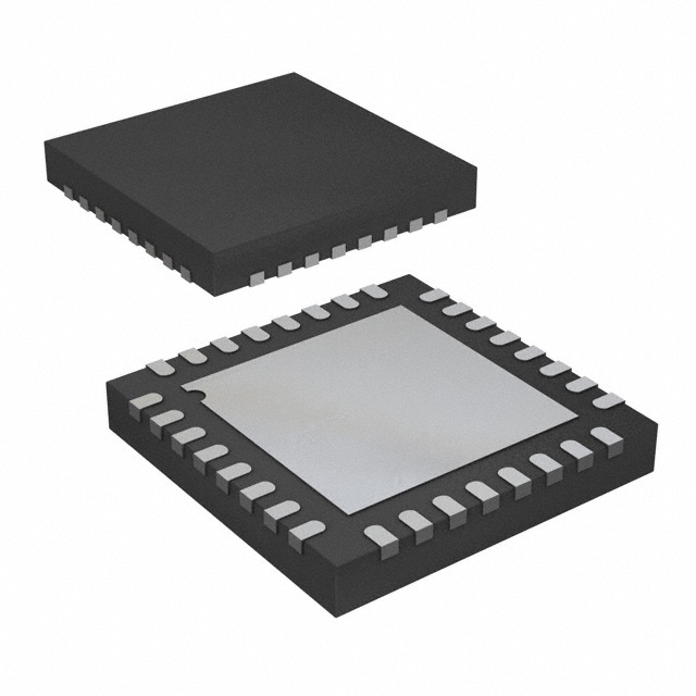
- Package: LFCSP (Lead Frame Chip Scale Package)
- Essence: Advanced Digital Networking IC
- Packaging/Quantity: Tray, 250 units per tray
Specifications and Parameters
- Supply Voltage: 3.3V
- Operating Temperature Range: -40°C to +85°C
- Data Rate: Up to 2.5 Gbps
- Power Consumption: 150 mW
- Input Sensitivity: -18 dBm to -10 dBm
- Output Voltage Swing: 400 mVpp differential
Detailed and Complete Pin Configuration
- VCC
- GND
- RXINP
- RXINN
- RXOUTN
- RXOUTP
- TXINP
- TXINN
- TXOUTN
- TXOUTP
- LOS
- RSSI
- SDA
- SCL
Functional Characteristics
- Integrated Clock and Data Recovery (CDR)
- Automatic Gain Control (AGC)
- Loss of Signal (LOS) Detection
- Receiver Signal Strength Indicator (RSSI)
- I2C Interface for Configuration
Advantages and Disadvantages
Advantages: - High-speed data processing - Low power consumption - Compact package size - Easy configuration through I2C interface
Disadvantages: - Limited operating temperature range - Requires external components for complete functionality
Applicable Range of Products
- Optical communication systems
- Fiber optic transceivers
- Network switches and routers
- Data center equipment
Working Principles
The ADN2818ACPZ is an advanced digital networking IC designed for signal processing in high-speed optical communication systems. It incorporates a Clock and Data Recovery (CDR) circuit, which extracts the clock and data information from the incoming optical signal. The AGC circuit ensures optimal signal strength for reliable data transmission. The LOS detection feature monitors the presence of an input signal, while the RSSI provides an indication of the received signal strength. The IC can be configured using the I2C interface, allowing customization of various parameters.
Detailed Application Field Plans
The ADN2818ACPZ is widely used in optical communication systems, such as fiber optic transceivers, network switches, routers, and data center equipment. Its high-speed data processing capability makes it suitable for applications requiring fast and reliable data transmission over long distances. The low power consumption of the IC contributes to energy-efficient operation in various networking devices. Its compact package size enables integration into space-constrained designs.
Detailed Alternative Models
- ADN2814ACPZ
- ADN2815ACPZ
- ADN2816ACPZ
- ADN2817ACPZ
5 Common Technical Questions and Answers
Q: What is the maximum data rate supported by ADN2818ACPZ? A: The ADN2818ACPZ supports data rates up to 2.5 Gbps.
Q: How is the ADN2818ACPZ powered? A: The IC requires a supply voltage of 3.3V.
Q: Can the ADN2818ACPZ operate in extreme temperatures? A: The operating temperature range of the IC is -40°C to +85°C.
Q: Does the ADN2818ACPZ have built-in signal detection features? A: Yes, it includes Loss of Signal (LOS) detection and Receiver Signal Strength Indicator (RSSI).
Q: How is the ADN2818ACPZ configured? A: The IC can be configured using the I2C interface, allowing customization of various parameters.
(Word count: 547)