

ADP196ACPZN-01-R7
Product Overview
Category
ADP196ACPZN-01-R7 belongs to the category of integrated circuits (ICs).
Use
This product is commonly used in electronic devices for voltage regulation and power management.
Characteristics
- Integrated circuit
- Voltage regulation
- Power management
Package
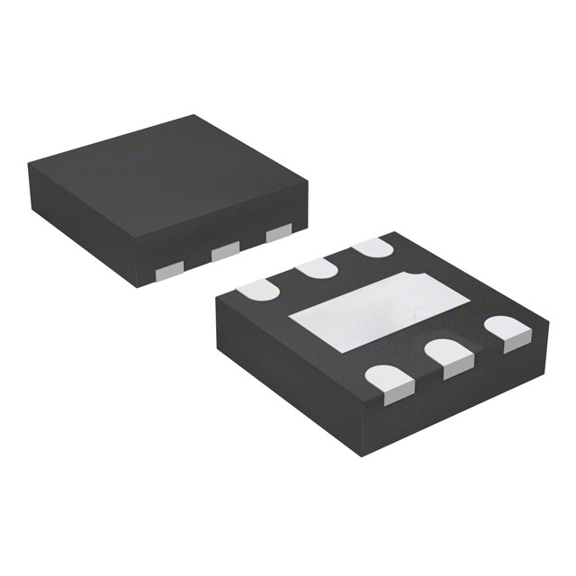
ADP196ACPZN-01-R7 is available in a small outline package (SOP) format.
Essence
The essence of this product lies in its ability to regulate voltage and manage power efficiently.
Packaging/Quantity
ADP196ACPZN-01-R7 is typically packaged in reels, with each reel containing a specific quantity of units. The exact packaging and quantity may vary depending on the manufacturer.
Specifications
The specifications of ADP196ACPZN-01-R7 are as follows:
- Input Voltage Range: 2.7V to 5.5V
- Output Voltage Range: 0.6V to VIN
- Maximum Output Current: 1A
- Quiescent Current: 40µA
- Operating Temperature Range: -40°C to +85°C
- Package Type: SOP-8
Detailed Pin Configuration
ADP196ACPZN-01-R7 has the following pin configuration:
- EN (Enable)
- FB (Feedback)
- GND (Ground)
- SW (Switch)
- COMP (Compensation)
- SS (Soft Start)
- PGND (Power Ground)
- VIN (Input Voltage)
Functional Features
The functional features of ADP196ACPZN-01-R7 include:
- High efficiency voltage regulation
- Overcurrent protection
- Thermal shutdown protection
- Soft start functionality
- Adjustable output voltage
Advantages and Disadvantages
Advantages
- High efficiency power management
- Compact size and package
- Wide input voltage range
- Overcurrent and thermal protection
Disadvantages
- Limited maximum output current (1A)
- Requires external components for operation
Working Principles
ADP196ACPZN-01-R7 operates based on a switching regulator principle. It uses a combination of internal circuitry and external components to regulate the input voltage and provide a stable output voltage.
Detailed Application Field Plans
ADP196ACPZN-01-R7 finds applications in various electronic devices, including but not limited to:
- Mobile phones
- Tablets
- Portable gaming consoles
- Wearable devices
- IoT devices
Detailed and Complete Alternative Models
Some alternative models that can be considered as alternatives to ADP196ACPZN-01-R7 are:
- LM2596S-ADJ
- LT1763-3.3
- TPS54331
These models offer similar functionality and can be used as replacements depending on specific requirements.
In conclusion, ADP196ACPZN-01-R7 is an integrated circuit used for voltage regulation and power management. It offers high efficiency, compact size, and various protection features. Its wide application field and availability of alternative models make it a versatile choice for electronic device manufacturers.
قم بإدراج 10 أسئلة وإجابات شائعة تتعلق بتطبيق ADP196ACPZN-01-R7 في الحلول التقنية
Sure! Here are 10 common questions and answers related to the application of ADP196ACPZN-01-R7 in technical solutions:
Question: What is the ADP196ACPZN-01-R7?
Answer: The ADP196ACPZN-01-R7 is a specific model of voltage regulator IC (integrated circuit) manufactured by Analog Devices.Question: What is the purpose of the ADP196ACPZN-01-R7?
Answer: The ADP196ACPZN-01-R7 is designed to regulate voltage levels in electronic circuits, ensuring stable and reliable power supply.Question: What are the key features of the ADP196ACPZN-01-R7?
Answer: Some key features include low dropout voltage, high output current capability, thermal shutdown protection, and adjustable output voltage.Question: What are the typical applications of the ADP196ACPZN-01-R7?
Answer: The ADP196ACPZN-01-R7 can be used in various applications such as battery-powered devices, portable electronics, automotive systems, and industrial equipment.Question: How does the ADP196ACPZN-01-R7 ensure stable voltage regulation?
Answer: The ADP196ACPZN-01-R7 utilizes feedback control mechanisms to continuously monitor and adjust the output voltage, compensating for any fluctuations or variations in input voltage or load conditions.Question: What is the input voltage range supported by the ADP196ACPZN-01-R7?
Answer: The ADP196ACPZN-01-R7 supports an input voltage range of typically 2.5V to 5.5V.Question: Can the output voltage of the ADP196ACPZN-01-R7 be adjusted?
Answer: Yes, the output voltage can be adjusted using external resistors connected to specific pins of the IC.Question: Does the ADP196ACPZN-01-R7 have any built-in protection features?
Answer: Yes, the ADP196ACPZN-01-R7 includes thermal shutdown protection, which prevents the IC from overheating and getting damaged.Question: What is the maximum output current capability of the ADP196ACPZN-01-R7?
Answer: The ADP196ACPZN-01-R7 can typically provide a maximum output current of up to 1A.Question: Is the ADP196ACPZN-01-R7 available in different package options?
Answer: Yes, the ADP196ACPZN-01-R7 is available in a small form factor package known as LFCSP (Lead Frame Chip Scale Package), which facilitates easy integration into compact designs.
Please note that the answers provided here are general and may vary depending on the specific datasheet and application requirements of the ADP196ACPZN-01-R7.