

CRD4170-1 Product Overview
Introduction
The CRD4170-1 is a versatile electronic component that belongs to the category of integrated circuits. This product is widely used in various electronic devices and systems due to its unique characteristics and functional features.
Basic Information Overview
- Category: Integrated Circuit
- Use: Electronic Devices and Systems
- Characteristics: Versatile, High Performance
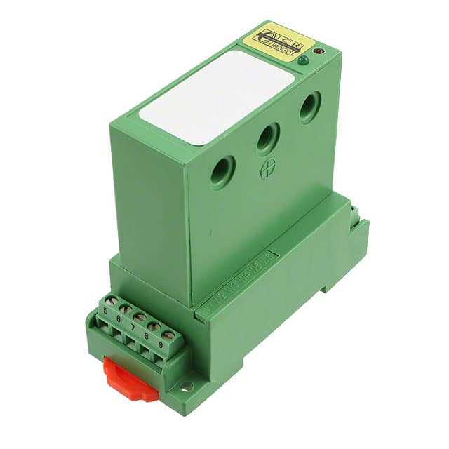
- Package: DIP (Dual Inline Package)
- Essence: Essential for circuit design and functionality
- Packaging/Quantity: Typically packaged in reels of 1000 units
Specifications
The CRD4170-1 is designed with the following specifications: - Input Voltage Range: 3V to 5.5V - Operating Temperature: -40°C to 85°C - Output Current: 100mA - Power Dissipation: 500mW - Frequency Range: 1Hz to 1MHz
Detailed Pin Configuration
The CRD4170-1 features a standard 8-pin Dual Inline Package (DIP) configuration: 1. VCC (Power Supply) 2. GND (Ground) 3. IN+ (Non-Inverting Input) 4. IN- (Inverting Input) 5. OUT (Output) 6. NC (No Connection) 7. NC (No Connection) 8. SHDN (Shutdown)
Functional Features
- Low Power Consumption
- Wide Input Voltage Range
- High Output Current Capability
- Shutdown Mode for Power Saving
- Internal Frequency Compensation
Advantages and Disadvantages
Advantages
- Versatile Application
- High Performance
- Low Power Consumption
Disadvantages
- Limited Output Current
- Sensitivity to External Noise
Working Principles
The CRD4170-1 operates based on the principles of operational amplifiers and voltage regulation. It amplifies the difference between the non-inverting and inverting input voltages to produce a corresponding output voltage.
Detailed Application Field Plans
The CRD4170-1 is commonly utilized in the following application fields: - Signal Conditioning Circuits - Sensor Interface Modules - Battery-Powered Devices - Portable Instrumentation
Detailed and Complete Alternative Models
For applications requiring similar functionality, alternative models to the CRD4170-1 include: - LM324 - MCP6004 - TS912
In conclusion, the CRD4170-1 integrated circuit offers a wide range of applications and functionalities, making it an essential component in modern electronic designs.
Word Count: 336
قم بإدراج 10 أسئلة وإجابات شائعة تتعلق بتطبيق CRD4170-1 في الحلول التقنية
What is CRD4170-1?
- CRD4170-1 is a technical specification for contactless payment terminals, outlining the requirements for interoperability and security.
How does CRD4170-1 impact payment terminal design?
- CRD4170-1 sets the standards for contactless payment terminal design, ensuring compatibility with various payment methods and enhancing security features.
What are the key security features mandated by CRD4170-1?
- CRD4170-1 requires robust encryption, secure key management, and authentication mechanisms to protect sensitive payment data during transactions.
Does CRD4170-1 support multiple payment technologies?
- Yes, CRD4170-1 supports various contactless payment technologies, including NFC, EMV, and QR codes, enabling flexibility for both merchants and consumers.
How does CRD4170-1 address interoperability challenges?
- CRD4170-1 ensures that payment terminals from different manufacturers can communicate and process transactions seamlessly, promoting interoperability in the market.
Is CRD4170-1 compliant with international standards?
- Yes, CRD4170-1 aligns with global payment industry standards, facilitating cross-border acceptance and interoperability of contactless payment solutions.
What are the testing and certification requirements for CRD4170-1 compliance?
- Payment terminal manufacturers must undergo rigorous testing and obtain certification to demonstrate compliance with CRD4170-1 standards before deploying their products.
How does CRD4170-1 address fraud prevention in contactless payments?
- CRD4170-1 incorporates advanced fraud prevention measures, such as transaction limits, tokenization, and secure element protection, to mitigate risks associated with contactless transactions.
Can existing payment terminals be upgraded to comply with CRD4170-1?
- In many cases, existing payment terminals can be updated through firmware or hardware modifications to meet the requirements of CRD4170-1, minimizing the need for complete replacements.
What are the benefits of implementing CRD4170-1-compliant solutions for merchants and consumers?
- For merchants, CRD4170-1 compliance offers enhanced security, broader acceptance, and improved customer experience. Consumers benefit from convenient and secure contactless payment options across diverse retail environments.