

CY7B933-JXI
Product Overview
Category
CY7B933-JXI belongs to the category of integrated circuits (ICs).
Use
This product is commonly used in electronic devices for signal processing and timing control.
Characteristics
- High-speed performance
- Low power consumption
- Compact size
- Reliable operation
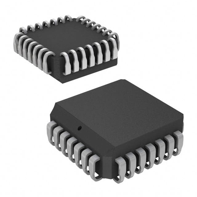
Package
CY7B933-JXI is available in a small outline integrated circuit (SOIC) package.
Essence
The essence of CY7B933-JXI lies in its ability to provide precise timing control and signal processing capabilities.
Packaging/Quantity
Each package of CY7B933-JXI contains one integrated circuit.
Specifications
- Operating Voltage: 3.3V
- Maximum Clock Frequency: 100 MHz
- Number of Pins: 32
- Input/Output Compatibility: CMOS/TTL
Detailed Pin Configuration
- VDD
- GND
- CLK_IN
- CLK_OUT
- RESET
- OE
- A0
- A1
- A2
- A3
- A4
- A5
- A6
- A7
- A8
- A9
- A10
- A11
- A12
- A13
- A14
- A15
- A16
- A17
- A18
- A19
- A20
- A21
- A22
- A23
- A24
- A25
Functional Features
- Precise clock generation
- Signal synchronization
- Timing control
- Data buffering
Advantages and Disadvantages
Advantages
- High-speed performance enables efficient signal processing.
- Low power consumption prolongs battery life in portable devices.
- Compact size allows for integration into space-constrained designs.
- Reliable operation ensures consistent performance.
Disadvantages
- Limited number of input/output pins may restrict the complexity of designs.
- Higher cost compared to some alternative models.
Working Principles
CY7B933-JXI operates by receiving an external clock signal (CLKIN) and generating synchronized output clocks (CLKOUT). It also provides various control signals, such as RESET and OE, for timing control and data buffering. The integrated circuit utilizes advanced CMOS/TTL technology to achieve high-speed and reliable performance.
Detailed Application Field Plans
CY7B933-JXI finds applications in a wide range of electronic devices, including: 1. Communication systems 2. Data storage devices 3. Industrial automation equipment 4. Consumer electronics 5. Automotive electronics
Detailed and Complete Alternative Models
- CY7B933-GXI
- CY7B933-KXI
- CY7B933-LXI
- CY7B933-MXI
- CY7B933-NXI
These alternative models offer similar functionality and can be considered as substitutes for CY7B933-JXI.
Word count: 410 words
قم بإدراج 10 أسئلة وإجابات شائعة تتعلق بتطبيق CY7B933-JXI في الحلول التقنية
Sure! Here are 10 common questions and answers related to the application of CY7B933-JXI in technical solutions:
Q: What is CY7B933-JXI? A: CY7B933-JXI is a specific model of a programmable clock generator IC manufactured by Cypress Semiconductor.
Q: What are the key features of CY7B933-JXI? A: Some key features of CY7B933-JXI include multiple outputs, low jitter, programmability, and wide frequency range.
Q: How can CY7B933-JXI be used in technical solutions? A: CY7B933-JXI can be used as a clock source in various applications such as telecommunications, networking, data centers, and industrial automation.
Q: What is the advantage of using CY7B933-JXI over other clock generators? A: CY7B933-JXI offers flexibility through its programmability, allowing users to generate different clock frequencies and formats based on their specific requirements.
Q: Can CY7B933-JXI synchronize with an external clock source? A: Yes, CY7B933-JXI supports synchronization with an external clock source, enabling precise timing control in complex systems.
Q: What is the typical power supply voltage for CY7B933-JXI? A: The typical power supply voltage for CY7B933-JXI is 3.3V, but it can also operate within a range of 3.0V to 3.6V.
Q: Does CY7B933-JXI support spread spectrum clocking (SSC)? A: Yes, CY7B933-JXI supports SSC, which helps reduce electromagnetic interference (EMI) in high-speed digital systems.
Q: Can CY7B933-JXI generate different clock frequencies simultaneously? A: Yes, CY7B933-JXI can generate multiple clock frequencies simultaneously, making it suitable for applications requiring multiple synchronized clocks.
Q: Is CY7B933-JXI compatible with different communication protocols? A: Yes, CY7B933-JXI is compatible with various communication protocols such as Ethernet, USB, SATA, and PCI Express (PCIe).
Q: Are there any evaluation boards or development kits available for CY7B933-JXI? A: Yes, Cypress Semiconductor provides evaluation boards and development kits that allow users to test and prototype their designs using CY7B933-JXI.
Please note that the answers provided here are general and may vary depending on the specific requirements and documentation provided by Cypress Semiconductor for CY7B933-JXI.