

CY7C4201V-15AXC
Product Overview
Category
The CY7C4201V-15AXC belongs to the category of integrated circuits (ICs), specifically a synchronous dual-port static random access memory (SDRAM) chip.
Use
This chip is primarily used in electronic devices that require high-speed data storage and retrieval capabilities. It serves as a key component in various applications, including telecommunications equipment, networking devices, and embedded systems.
Characteristics
The CY7C4201V-15AXC offers several notable characteristics that make it suitable for demanding data-intensive tasks. It operates at a clock frequency of 133 MHz and has a capacity of 4 megabits (512 kilobytes). The chip supports simultaneous read and write operations, enabling efficient data transfer. Additionally, it features low power consumption and a wide operating temperature range.
Package
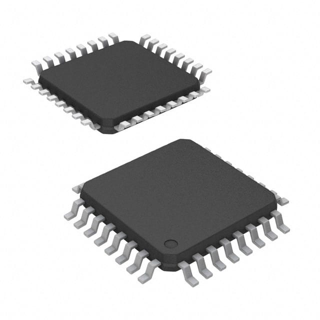
The CY7C4201V-15AXC is available in a compact and industry-standard 44-pin TSOP-II package. This package ensures easy integration into circuit boards and provides reliable electrical connections.
Essence
At its core, the CY7C4201V-15AXC is designed to provide fast and reliable data storage and retrieval capabilities. Its essence lies in its ability to handle high-speed data transfers while maintaining data integrity and stability.
Packaging/Quantity
The CY7C4201V-15AXC is typically packaged in reels or tubes, depending on the manufacturer's preference. Each reel or tube contains a specific quantity of chips, usually ranging from hundreds to thousands, depending on customer requirements.
Specifications
- Clock Frequency: 133 MHz
- Capacity: 4 Megabits (512 Kilobytes)
- Operating Voltage: 3.3 Volts
- Operating Temperature Range: -40°C to +85°C
- Package Type: 44-pin TSOP-II
Detailed Pin Configuration
The CY7C4201V-15AXC features a 44-pin configuration, with each pin serving a specific purpose. The detailed pin configuration is as follows:
(Pin Number) (Pin Name) - (Description) 1 - VDDQ - Power Supply for I/O Buffers 2 - DQ0 - Data Input/Output Bit 0 3 - DQ1 - Data Input/Output Bit 1 4 - DQ2 - Data Input/Output Bit 2 5 - DQ3 - Data Input/Output Bit 3 6 - DQ4 - Data Input/Output Bit 4 7 - DQ5 - Data Input/Output Bit 5 8 - DQ6 - Data Input/Output Bit 6 9 - DQ7 - Data Input/Output Bit 7 10 - VSSQ - Ground for I/O Buffers 11 - WE# - Write Enable 12 - CAS# - Column Address Strobe 13 - RAS# - Row Address Strobe 14 - A0 - Address Bit 0 15 - A1 - Address Bit 1 16 - A2 - Address Bit 2 17 - A3 - Address Bit 3 18 - A4 - Address Bit 4 19 - A5 - Address Bit 5 20 - A6 - Address Bit 6 21 - A7 - Address Bit 7 22 - A8 - Address Bit 8 23 - A9 - Address Bit 9 24 - A10 - Address Bit 10 25 - A11 - Address Bit 11 26 - A12 - Address Bit 12 27 - A13 - Address Bit 13 28 - A14 - Address Bit 14 29 - A15 - Address Bit 15 30 - VDD - Power Supply 31 - DQ15 - Data Input/Output Bit 15 32 - DQ14 - Data Input/Output Bit 14 33 - DQ13 - Data Input/Output Bit 13 34 - DQ12 - Data Input/Output Bit 12 35 - DQ11 - Data Input/Output Bit 11 36 - DQ10 - Data Input/Output Bit 10 37 - DQ9 - Data Input/Output Bit 9 38 - DQ8 - Data Input/Output Bit 8 39 - VSS - Ground 40 - CLK - Clock Input 41 - OE# - Output Enable 42 - LB# - Lower Byte Control 43 - UB# - Upper Byte Control 44 - VDDQ - Power Supply for I/O Buffers
Functional Features
The CY7C4201V-15AXC offers several functional features that enhance its performance and usability. These include:
Simultaneous Read and Write Operations: The chip allows for concurrent read and write operations, enabling efficient data transfer and manipulation.
Low
قم بإدراج 10 أسئلة وإجابات شائعة تتعلق بتطبيق CY7C4201V-15AXC في الحلول التقنية
Sure! Here are 10 common questions and answers related to the application of CY7C4201V-15AXC in technical solutions:
Q1: What is CY7C4201V-15AXC? A1: CY7C4201V-15AXC is a specific model of synchronous SRAM (Static Random Access Memory) manufactured by Cypress Semiconductor. It has a capacity of 256K (32K x 8) and operates at a speed of 15ns.
Q2: What are the typical applications of CY7C4201V-15AXC? A2: CY7C4201V-15AXC is commonly used in various technical solutions such as networking equipment, telecommunications systems, industrial automation, medical devices, and automotive electronics.
Q3: What is the voltage requirement for CY7C4201V-15AXC? A3: CY7C4201V-15AXC operates at a voltage range of 4.5V to 5.5V.
Q4: Can CY7C4201V-15AXC be used in battery-powered devices? A4: Yes, CY7C4201V-15AXC can be used in battery-powered devices as long as the voltage requirement of 4.5V to 5.5V is met.
Q5: Does CY7C4201V-15AXC support multiple read and write operations simultaneously? A5: No, CY7C4201V-15AXC is a synchronous SRAM and does not support simultaneous multiple read or write operations.
Q6: What is the operating temperature range for CY7C4201V-15AXC? A6: CY7C4201V-15AXC has an operating temperature range of -40°C to +85°C.
Q7: Can CY7C4201V-15AXC be used in high-speed data processing applications? A7: Yes, CY7C4201V-15AXC operates at a speed of 15ns, which makes it suitable for many high-speed data processing applications.
Q8: Does CY7C4201V-15AXC have any power-saving features? A8: No, CY7C4201V-15AXC does not have specific power-saving features. However, it consumes low power during standby mode.
Q9: Is CY7C4201V-15AXC compatible with other SRAM devices? A9: Yes, CY7C4201V-15AXC is compatible with other SRAM devices that have similar voltage requirements and interface specifications.
Q10: Are there any specific design considerations when using CY7C4201V-15AXC? A10: When designing with CY7C4201V-15AXC, it is important to consider signal integrity, proper decoupling capacitors, and adherence to the recommended operating conditions provided in the datasheet.
Please note that these answers are general and may vary depending on the specific requirements and application context. It is always recommended to refer to the datasheet and consult with Cypress Semiconductor or technical experts for accurate information.