

Encyclopedia Entry: 74AUP2G3404FW3-7
Product Overview
Category
The 74AUP2G3404FW3-7 belongs to the category of integrated circuits (ICs).
Use
This IC is commonly used in electronic devices for signal switching and amplification.
Characteristics
- Low power consumption
- High-speed operation
- Small package size
- Wide operating voltage range
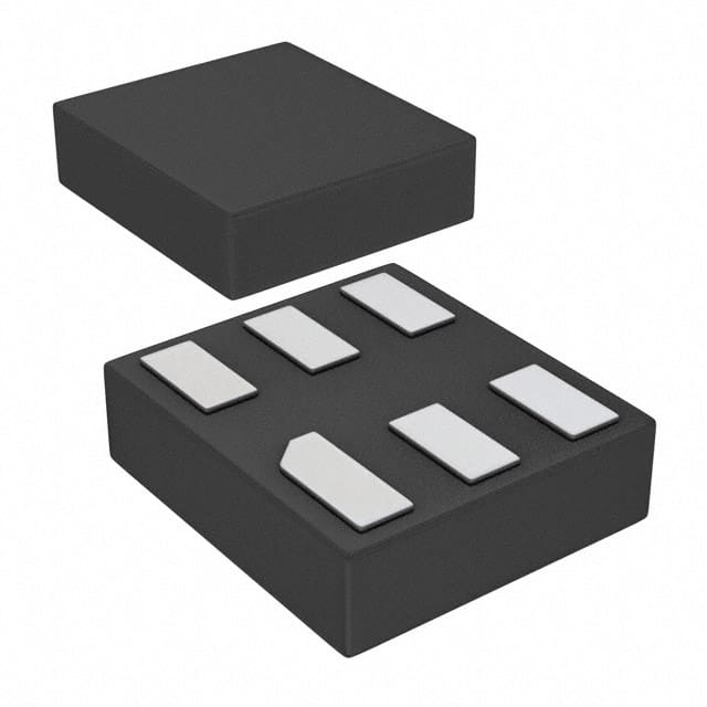
Package
The 74AUP2G3404FW3-7 is available in a small form factor package, such as a flip-chip or wafer-level chip-scale package (WLCSP).
Essence
The essence of this product lies in its ability to provide efficient signal switching and amplification while consuming minimal power.
Packaging/Quantity
The 74AUP2G3404FW3-7 is typically packaged in reels or trays, with quantities varying based on customer requirements.
Specifications
- Supply Voltage Range: 1.65V to 5.5V
- Operating Temperature Range: -40°C to +85°C
- Input Capacitance: 1.5pF (typical)
- Output Capacitance: 1.8pF (typical)
- Maximum Output Current: ±24mA
Detailed Pin Configuration
The 74AUP2G3404FW3-7 has a total of 6 pins, which are labeled as follows:
- VCC: Power supply input
- GND: Ground reference
- IN1: Input 1
- IN2: Input 2
- OUT: Output
- NC: No connection
Functional Features
- Dual-channel signal switching
- High-speed operation for quick response times
- Low power consumption for energy-efficient designs
- Wide operating voltage range for compatibility with various systems
Advantages and Disadvantages
Advantages
- Low power consumption extends battery life in portable devices.
- High-speed operation enables rapid signal switching.
- Small package size allows for compact circuit designs.
- Wide operating voltage range provides flexibility in system integration.
Disadvantages
- Limited output current may restrict use in high-power applications.
- Sensitivity to electrostatic discharge (ESD) requires proper handling during assembly.
Working Principles
The 74AUP2G3404FW3-7 operates based on complementary metal-oxide-semiconductor (CMOS) technology. It utilizes MOSFET transistors to control the flow of signals between its inputs and outputs. When an appropriate voltage is applied to the input pins, the IC switches the signal to the output pin, amplifying it if necessary.
Detailed Application Field Plans
The 74AUP2G3404FW3-7 finds application in various electronic systems, including but not limited to: - Mobile phones and smartphones - Tablets and laptops - Portable media players - Wearable devices - IoT (Internet of Things) devices - Automotive electronics
Detailed and Complete Alternative Models
- 74AUP2G3404SE-7: Similar specifications and features, but available in a different package.
- 74AUP2G3404GN-7: Offers enhanced ESD protection, suitable for more demanding environments.
- 74AUP2G3404FT3-7: Provides extended temperature range for extreme operating conditions.
These alternative models offer similar functionality and can be considered as substitutes for the 74AUP2G3404FW3-7 depending on specific requirements.
Word count: 536 words
قم بإدراج 10 أسئلة وإجابات شائعة تتعلق بتطبيق 74AUP2G3404FW3-7 في الحلول التقنية
Sure! Here are 10 common questions and answers related to the application of 74AUP2G3404FW3-7 in technical solutions:
Q: What is the function of the 74AUP2G3404FW3-7? A: The 74AUP2G3404FW3-7 is a dual buffer with Schmitt-trigger inputs, used for signal buffering and level shifting.
Q: What is the operating voltage range of the 74AUP2G3404FW3-7? A: The 74AUP2G3404FW3-7 operates within a voltage range of 0.8V to 3.6V.
Q: Can the 74AUP2G3404FW3-7 be used in both digital and analog applications? A: Yes, the 74AUP2G3404FW3-7 can be used in both digital and analog applications.
Q: What is the maximum output current of the 74AUP2G3404FW3-7? A: The 74AUP2G3404FW3-7 has a maximum output current of 32mA.
Q: Does the 74AUP2G3404FW3-7 have built-in ESD protection? A: Yes, the 74AUP2G3404FW3-7 has built-in ESD protection, making it more robust against electrostatic discharge.
Q: Can the 74AUP2G3404FW3-7 be used in high-speed applications? A: Yes, the 74AUP2G3404FW3-7 is suitable for high-speed applications with a propagation delay of only a few nanoseconds.
Q: What is the package type of the 74AUP2G3404FW3-7? A: The 74AUP2G3404FW3-7 is available in a small SOT353 package.
Q: Can the 74AUP2G3404FW3-7 be used in battery-powered devices? A: Yes, the 74AUP2G3404FW3-7 is suitable for battery-powered devices due to its low power consumption.
Q: Is the 74AUP2G3404FW3-7 compatible with other logic families? A: Yes, the 74AUP2G3404FW3-7 is compatible with various logic families, including CMOS and TTL.
Q: Are there any specific application notes or reference designs available for the 74AUP2G3404FW3-7? A: Yes, the manufacturer provides application notes and reference designs that can help in implementing the 74AUP2G3404FW3-7 in different technical solutions.
Please note that these answers are general and may vary depending on the specific requirements and use cases. It's always recommended to refer to the datasheet and consult with the manufacturer for detailed information.