

74LVC1G11W6-7
Product Overview
Category
The 74LVC1G11W6-7 belongs to the category of integrated circuits (ICs).
Use
This IC is commonly used in electronic devices for logic gate applications.
Characteristics
- Low-voltage CMOS technology
- High-speed operation
- Wide operating voltage range
- Low power consumption
- Small package size
Package
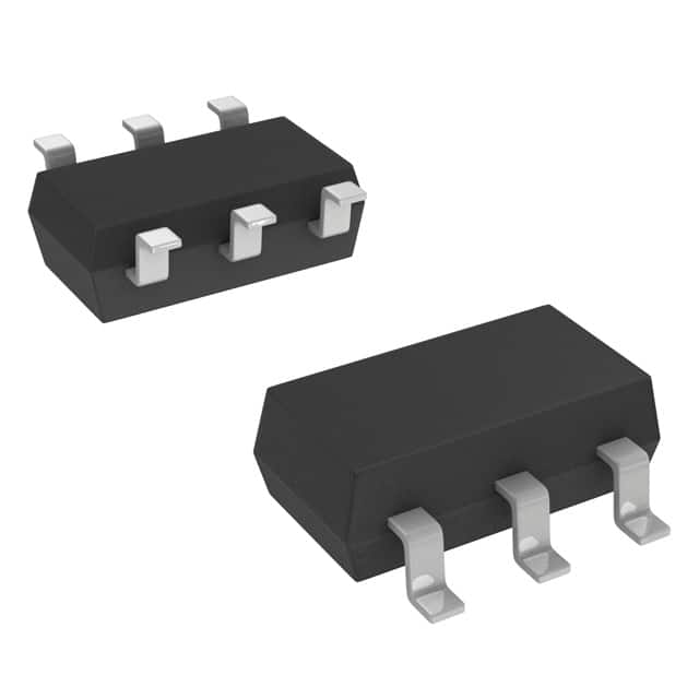
The 74LVC1G11W6-7 is available in a small SOT-353 package.
Essence
This IC is an AND gate that operates at low voltage levels, making it suitable for battery-powered devices and other low-power applications.
Packaging/Quantity
The 74LVC1G11W6-7 is typically packaged in reels or tubes, with a quantity of 3000 units per reel/tube.
Specifications
- Supply Voltage Range: 1.65V to 5.5V
- Input Voltage Range: 0V to VCC
- Output Voltage Range: 0V to VCC
- Operating Temperature Range: -40°C to +125°C
- Propagation Delay: 4.3 ns (typical)
- Maximum Quiescent Current: 2 μA
Detailed Pin Configuration
The 74LVC1G11W6-7 has the following pin configuration:
____
   A --|    |-- VCC
   B --|    |-- Y
GND/VSS --|____|-- GND/VSS
Functional Features
- Single-input AND gate functionality
- High-speed operation allows for efficient signal processing
- Wide operating voltage range enables compatibility with various systems
- Low power consumption helps conserve battery life in portable devices
Advantages and Disadvantages
Advantages
- Low-voltage operation makes it suitable for battery-powered devices
- Small package size allows for space-efficient designs
- High-speed operation enables efficient signal processing
Disadvantages
- Limited number of inputs (single-input AND gate)
- May not be suitable for complex logic operations requiring multiple inputs
Working Principles
The 74LVC1G11W6-7 is based on low-voltage CMOS technology. It operates as a single-input AND gate, where the output is high only when both inputs are high. The IC utilizes transistors and logic gates to perform the logical AND operation.
Detailed Application Field Plans
The 74LVC1G11W6-7 can be used in various applications, including but not limited to: - Battery-powered devices - Portable electronics - Consumer electronics - Industrial automation - Automotive systems
Detailed and Complete Alternative Models
Some alternative models that offer similar functionality to the 74LVC1G11W6-7 include: - 74HC1G08: Single-input AND gate with open-drain output - 74LS08: Quad 2-input AND gate - SN74LVC1G08: Single-input AND gate with Schmitt-trigger input
These alternative models provide different features and specifications, allowing designers to choose the most suitable option for their specific requirements.
Word count: 470 words
قم بإدراج 10 أسئلة وإجابات شائعة تتعلق بتطبيق 74LVC1G11W6-7 في الحلول التقنية
Sure! Here are 10 common questions and answers related to the application of the 74LVC1G11W6-7 in technical solutions:
1. What is the 74LVC1G11W6-7? - The 74LVC1G11W6-7 is a single 3-input AND gate IC (integrated circuit) that operates at a voltage level of 1.65V to 5.5V.
2. What is the purpose of the 74LVC1G11W6-7? - The purpose of this IC is to perform logical AND operations on three input signals, providing a single output signal based on the inputs' logic levels.
3. What are the typical applications of the 74LVC1G11W6-7? - This IC is commonly used in various digital systems, such as microcontrollers, FPGA (Field-Programmable Gate Array) designs, communication devices, and other electronic circuits requiring logical AND functionality.
4. What is the maximum operating frequency of the 74LVC1G11W6-7? - The maximum operating frequency of this IC is typically around 200 MHz.
5. What is the power supply voltage range for the 74LVC1G11W6-7? - The power supply voltage range for this IC is from 1.65V to 5.5V.
6. How many pins does the 74LVC1G11W6-7 have? - The 74LVC1G11W6-7 has a total of 6 pins.
7. What is the pin configuration of the 74LVC1G11W6-7? - Pin 1: Input A - Pin 2: Input B - Pin 3: Input C - Pin 4: Ground (GND) - Pin 5: Output (Y) - Pin 6: Power Supply (VCC)
8. What is the output logic level of the 74LVC1G11W6-7? - The output logic level of this IC is compatible with both CMOS and TTL logic levels.
9. Can the 74LVC1G11W6-7 be used in high-speed applications? - Yes, this IC is designed to operate at high speeds, making it suitable for use in high-speed digital systems.
10. Is the 74LVC1G11W6-7 available in different package types? - Yes, this IC is available in various package types, including SOT-23, SC-70, and XSON6.