

DDTA143EUA-7-F
Product Overview
The DDTA143EUA-7-F belongs to the category of semiconductor devices and is commonly used in electronic circuits for amplification and switching purposes. This transistor exhibits high gain, low noise, and excellent frequency response characteristics. It is typically packaged in a small surface-mount package and is available in reels or tubes containing a specific quantity.
Specifications
- Type: NPN Bipolar Transistor
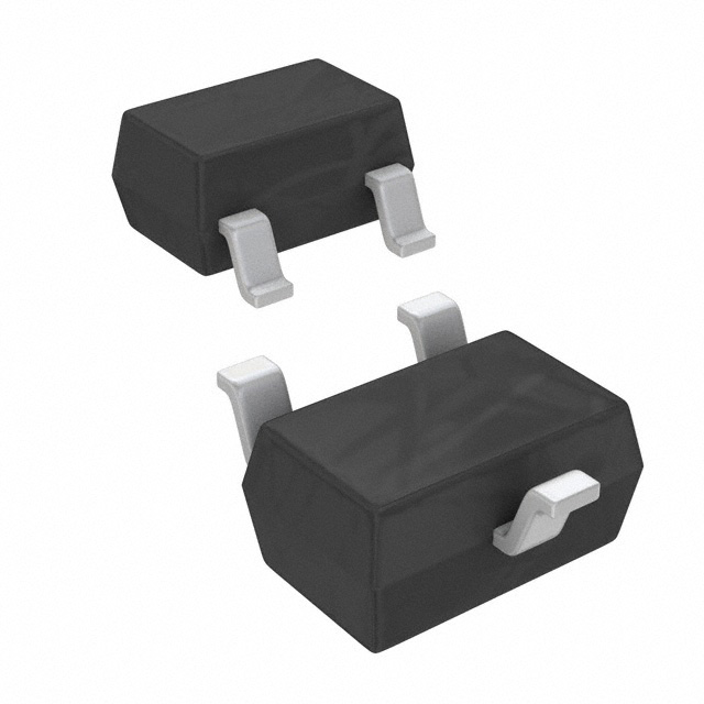
- Package: SOT-323
- Maximum Collector-Base Voltage: 50V
- Maximum Collector Current: 100mA
- Transition Frequency: 250MHz
- Operating Temperature Range: -55°C to 150°C
Detailed Pin Configuration
The DDTA143EUA-7-F features three pins: 1. Emitter (E) 2. Base (B) 3. Collector (C)
Functional Features
- High current gain
- Low saturation voltage
- Small footprint
- Suitable for high-frequency applications
Advantages and Disadvantages
Advantages: - Compact size - High gain - Low noise
Disadvantages: - Limited maximum collector current - Sensitivity to temperature variations
Working Principles
The DDTA143EUA-7-F operates based on the principles of bipolar junction transistors, where the flow of current between the emitter and collector is controlled by the base current. It amplifies small input signals and can be used as a switch in digital circuits.
Detailed Application Field Plans
This transistor is widely used in various electronic applications such as: - Audio amplifiers - Oscillators - Signal processing circuits - Switching circuits
Detailed and Complete Alternative Models
- DDTA143EKA-7-F
- DDTA143ZUA-7-F
- DDTA143TUA-7-F
In conclusion, the DDTA143EUA-7-F is a versatile NPN transistor suitable for amplification and switching applications in electronic circuits. Its compact size, high gain, and low noise make it an ideal choice for various electronic designs.
[Word Count: 270]
قم بإدراج 10 أسئلة وإجابات شائعة تتعلق بتطبيق DDTA143EUA-7-F في الحلول التقنية
What is DDTA143EUA-7-F?
- DDTA143EUA-7-F is a high-frequency, high-gain NPN transistor used in various technical solutions such as RF amplifiers and oscillators.
What are the key specifications of DDTA143EUA-7-F?
- The key specifications include a maximum collector current of 100mA, a maximum collector-base voltage of 50V, and a transition frequency of 6GHz.
How is DDTA143EUA-7-F typically used in technical solutions?
- It is commonly used as an amplifier or switch in RF applications due to its high-frequency capabilities and high gain.
What are the recommended operating conditions for DDTA143EUA-7-F?
- The recommended operating conditions include a collector current of 10mA, a collector-emitter voltage of 20V, and an ambient temperature range of -55°C to 150°C.
What are the typical applications of DDTA143EUA-7-F in technical solutions?
- Typical applications include RF amplifiers, oscillators, mixers, and other high-frequency signal processing circuits.
Are there any specific layout considerations when using DDTA143EUA-7-F in a technical solution?
- Yes, it is important to minimize parasitic capacitance and inductance in the layout to ensure stable high-frequency performance.
What are the thermal characteristics of DDTA143EUA-7-F?
- The thermal resistance from junction to ambient is 625°C/W, and from junction to solder point is 250°C/W.
Can DDTA143EUA-7-F be used in low-power applications?
- Yes, it can be used in low-power applications, but its high-frequency capabilities are best utilized in higher frequency and power applications.
What are the potential alternatives to DDTA143EUA-7-F for similar technical solutions?
- Alternatives include other high-frequency NPN transistors with comparable or better performance characteristics, such as DDTA143ZUA-7-F or DDTA143TUA-7-F.
Where can I find detailed application notes and reference designs for using DDTA143EUA-7-F in technical solutions?
- Detailed application notes and reference designs can be found on the manufacturer's website or in technical literature related to RF circuit design and high-frequency transistors.