

PI6C4911505-07LIEX
Overview
- Category: Integrated Circuit
- Use: Clock Generator and Buffer
- Characteristics: Low jitter, high frequency accuracy, low power consumption
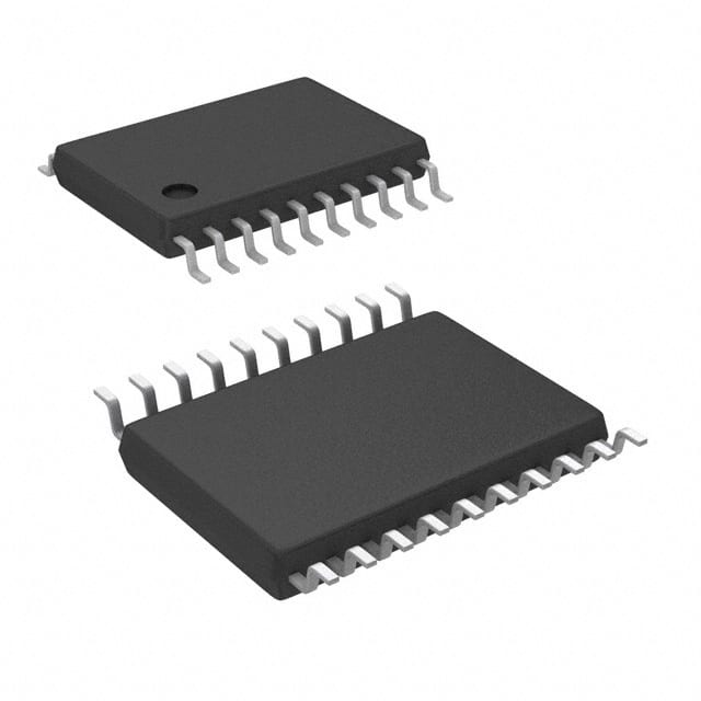
- Package: 48-pin LQFP
- Essence: Clock generation and buffering for electronic devices
- Packaging/Quantity: Tape and Reel, 250 units per reel
Specifications and Parameters
- Input Voltage Range: 2.7V to 3.6V
- Output Frequency Range: 1MHz to 200MHz
- Operating Temperature Range: -40°C to +85°C
- Supply Current: 20mA (typical)
- Output Type: LVCMOS
Pin Configuration
The PI6C4911505-07LIEX has a total of 48 pins. The pin configuration is as follows:
- VDD
- GND
- OUT0
- OUT1
- OUT2
- OUT3
- OUT4
- OUT5
- OUT6
- OUT7
- OUT8
- OUT9
- OUT10
- OUT11
- OUT12
- OUT13
- OUT14
- OUT15
- OUT16
- OUT17
- OUT18
- OUT19
- OUT20
- OUT21
- OUT22
- OUT23
- OUT24
- OUT25
- OUT26
- OUT27
- OUT28
- OUT29
- OUT30
- OUT31
- OUT32
- OUT33
- OUT34
- OUT35
- OUT36
- OUT37
- OUT38
- OUT39
- OUT40
- OUT41
- OUT42
- OUT43
- OUT44
- OUT45
Functional Characteristics
- Low jitter clock generation
- High frequency accuracy
- Programmable output frequencies
- Spread Spectrum Clocking (SSC) support
- Power management features for low power consumption
Advantages and Disadvantages
Advantages: - Low jitter ensures accurate timing in electronic devices - Wide range of programmable output frequencies - Power management features help reduce power consumption
Disadvantages: - Limited to LVCMOS output type - Requires external components for proper operation
Applicable Range of Products
The PI6C4911505-07LIEX is suitable for use in various electronic devices that require precise clock generation and buffering. It can be used in applications such as communication systems, data storage devices, and consumer electronics.
Working Principles
The PI6C4911505-07LIEX generates clock signals by utilizing an internal oscillator and frequency dividers. The generated clocks are then buffered and distributed to the output pins. The device also provides options for spread spectrum clocking to reduce electromagnetic interference.
Detailed Application Field Plans
- Communication Systems: Use the PI6C4911505-07LIEX to generate stable clock signals for data transmission and reception in communication systems.
- Data Storage Devices: Utilize the device to provide accurate timing for data reading and writing operations in storage devices such as hard drives and solid-state drives.
- Consumer Electronics: Incorporate the PI6C4911505-07LIEX into audio/video equipment, gaming consoles, and other consumer electronics to ensure precise synchronization and timing.
Detailed Alternative Models
- PI6C4911505-06LIEX: Similar to the PI6C4911505-07LIEX but with a different package type (40-pin QFN).
- PI6C4911505-08LIEX: Similar to the PI6C4911505-07LIEX but with extended temperature range (-40°C to +105°C).
5 Common Technical Questions and Answers
Q: What is the maximum output frequency of the PI6C4911505-07LIEX? A: The device can generate clock signals with frequencies up to 200MHz.
Q: Can I use this IC in a battery-powered device? A: Yes, the PI6C4911505-07LIEX has low power consumption and is suitable for battery-powered applications.
Q: Does the device support spread spectrum clocking? A: Yes, the PI6C4911505-07LIEX provides support for spread spectrum clocking to reduce electromagnetic interference.
Q: What is the operating voltage range of the IC? A: The device operates within a voltage range of 2.7V to 3.6V.
Q: Are there any alternative package options available? A: