

SP6651AER-L
Product Overview
- Category: Integrated Circuit
- Use: Power Management
- Characteristics: High Efficiency, Low Power Consumption
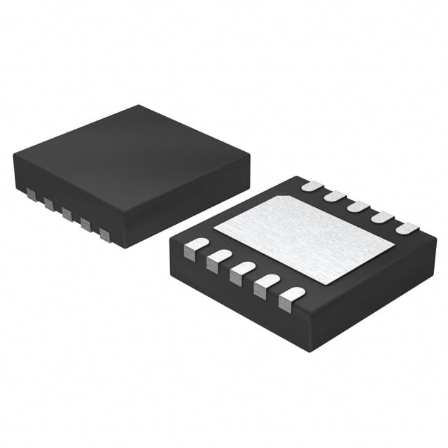
- Package: QFN (Quad Flat No-Lead)
- Essence: Regulates and controls power supply in electronic devices
- Packaging/Quantity: Tape and Reel, 2500 units per reel
Specifications
- Input Voltage Range: 2.7V to 5.5V
- Output Voltage Range: 0.6V to 3.3V
- Output Current: Up to 1.5A
- Operating Temperature Range: -40°C to +85°C
- Efficiency: Up to 95%
- Quiescent Current: 20µA (typical)
Detailed Pin Configuration
The SP6651AER-L has a total of 16 pins arranged as follows:
- VIN: Input voltage pin
- GND: Ground pin
- EN: Enable pin
- FB: Feedback pin
- VOUT: Output voltage pin
- COMP: Compensation pin
- SS: Soft-start pin
- PGND: Power ground pin
- BST: Boost pin
- SW: Switching pin
- AGND: Analog ground pin
- NC: Not connected
- NC: Not connected
- NC: Not connected
- NC: Not connected
- NC: Not connected
Functional Features
- High efficiency power conversion
- Low power consumption in standby mode
- Overcurrent protection
- Thermal shutdown protection
- Soft-start for smooth power-up
- Adjustable output voltage
- Stable and reliable performance
Advantages and Disadvantages
Advantages: - High efficiency leads to reduced power consumption - Wide input voltage range allows for versatile applications - Compact package size saves board space - Overcurrent and thermal protection ensure device safety - Soft-start feature prevents inrush current
Disadvantages: - Limited output current may not be suitable for high-power applications - Requires external components for proper operation - Higher cost compared to non-integrated solutions
Working Principles
The SP6651AER-L is a step-down (buck) DC-DC converter. It regulates the input voltage to a lower, stable output voltage using a switching regulator topology. The integrated circuit controls the duty cycle of the internal power switch to efficiently convert the input power to the desired output voltage. It employs a feedback mechanism to continuously monitor and adjust the output voltage, ensuring it remains within the specified range.
Detailed Application Field Plans
The SP6651AER-L is widely used in various electronic devices that require efficient power management. Some common application fields include:
- Mobile devices: Smartphones, tablets, portable media players
- IoT devices: Wearables, smart home devices, sensors
- Consumer electronics: Digital cameras, handheld gaming consoles
- Industrial equipment: Test and measurement instruments, control systems
- Automotive electronics: Infotainment systems, navigation devices
Detailed and Complete Alternative Models
- SP6650AER-L: Similar specifications and features, but with a different pin configuration.
- SP6652AER-L: Higher output current capability, suitable for more power-hungry applications.
- SP6649AER-L: Lower output voltage range, ideal for specific low-power applications.
- SP6651BER-L: Same specifications as SP6651AER-L, but in a different package (BGA instead of QFN).
These alternative models provide flexibility in choosing the most suitable solution based on specific requirements.
Word count: 452 words
قم بإدراج 10 أسئلة وإجابات شائعة تتعلق بتطبيق SP6651AER-L في الحلول التقنية
Sure! Here are 10 common questions and answers related to the application of SP6651AER-L in technical solutions:
Q1: What is SP6651AER-L? A1: SP6651AER-L is a specific model of a power management integrated circuit (PMIC) designed for use in various technical solutions.
Q2: What are the key features of SP6651AER-L? A2: Some key features of SP6651AER-L include multiple voltage regulators, power sequencing capabilities, fault protection mechanisms, and low power consumption.
Q3: What technical solutions can SP6651AER-L be used in? A3: SP6651AER-L can be used in a wide range of technical solutions such as smartphones, tablets, portable devices, IoT devices, and other battery-powered applications.
Q4: How many voltage regulators does SP6651AER-L have? A4: SP6651AER-L has multiple voltage regulators, typically including step-down (buck) regulators and/or step-up (boost) regulators.
Q5: Can SP6651AER-L handle different input voltages? A5: Yes, SP6651AER-L is designed to handle a wide range of input voltages, typically from a few volts up to several tens of volts.
Q6: Does SP6651AER-L support power sequencing? A6: Yes, SP6651AER-L has built-in power sequencing capabilities, allowing for controlled startup and shutdown of different power domains in a system.
Q7: What fault protection mechanisms does SP6651AER-L provide? A7: SP6651AER-L typically includes various fault protection features like overvoltage protection (OVP), undervoltage protection (UVP), overcurrent protection (OCP), and thermal shutdown.
Q8: Is SP6651AER-L suitable for low power applications? A8: Yes, SP6651AER-L is designed to be highly efficient and has low power consumption, making it suitable for battery-powered devices and other low power applications.
Q9: Can SP6651AER-L be used in automotive applications? A9: Yes, SP6651AER-L is often qualified for automotive-grade applications and can operate within the specified temperature range and meet the required standards.
Q10: Are evaluation boards or reference designs available for SP6651AER-L? A10: Yes, many manufacturers provide evaluation boards and reference designs that showcase the application of SP6651AER-L in different technical solutions, helping developers get started quickly.
Please note that the specific details and answers may vary depending on the manufacturer's documentation and specifications for SP6651AER-L.