

54FCT374ATDB
Product Overview
Category
The 54FCT374ATDB belongs to the category of integrated circuits (ICs).
Use
This IC is commonly used in digital systems for data storage and transfer applications.
Characteristics
- High-speed operation
- Low power consumption
- Wide operating voltage range
- Compatibility with various logic families
- Robustness against noise and interference
Package
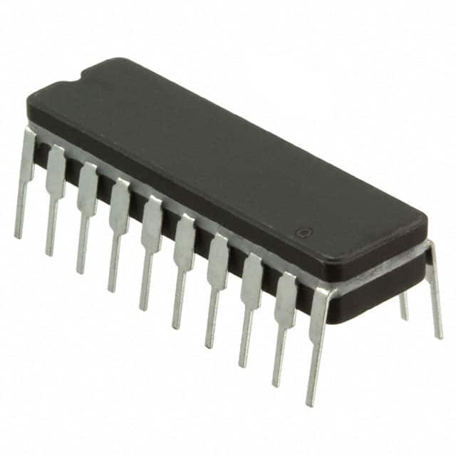
The 54FCT374ATDB is available in a standard dual in-line package (DIP) or surface mount package (SMD).
Essence
The essence of the 54FCT374ATDB lies in its ability to store and manipulate digital data efficiently and reliably.
Packaging/Quantity
The IC is typically packaged in reels or tubes, with quantities varying based on customer requirements.
Specifications
- Supply Voltage: 2.0V - 5.5V
- Operating Temperature Range: -40°C to +85°C
- Input/Output Logic Levels: TTL-compatible
- Maximum Clock Frequency: 100MHz
- Number of Flip-Flops: 8
- Output Drive Capability: 24mA
Detailed Pin Configuration
The 54FCT374ATDB has a total of 20 pins, each serving a specific function. The pin configuration is as follows:
- OE (Output Enable)
- D0 (Data Input 0)
- D1 (Data Input 1)
- D2 (Data Input 2)
- D3 (Data Input 3)
- D4 (Data Input 4)
- D5 (Data Input 5)
- D6 (Data Input 6)
- D7 (Data Input 7)
- GND (Ground)
- Q0 (Flip-Flop Output 0)
- Q1 (Flip-Flop Output 1)
- Q2 (Flip-Flop Output 2)
- Q3 (Flip-Flop Output 3)
- Q4 (Flip-Flop Output 4)
- Q5 (Flip-Flop Output 5)
- Q6 (Flip-Flop Output 6)
- Q7 (Flip-Flop Output 7)
- CLK (Clock Input)
- VCC (Supply Voltage)
Functional Features
- Data storage and transfer: The 54FCT374ATDB can store digital data in its flip-flops and transfer it to the output pins upon receiving a clock signal.
- Output enable control: The OE pin allows for enabling or disabling the output, providing flexibility in system design.
- High-speed operation: With a maximum clock frequency of 100MHz, this IC ensures efficient data processing in time-critical applications.
- Compatibility with various logic families: The 54FCT374ATDB is designed to work seamlessly with TTL and other compatible logic families, enhancing its versatility.
Advantages and Disadvantages
Advantages
- High-speed operation enables rapid data processing.
- Low power consumption contributes to energy efficiency.
- Wide operating voltage range allows for compatibility with different power supply systems.
- Robustness against noise and interference ensures reliable data transmission.
Disadvantages
- Limited number of flip-flops may restrict the complexity of data storage and manipulation.
- Availability in specific package types may limit integration options in certain systems.
Working Principles
The 54FCT374ATDB operates based on the principles of flip-flop circuits. When the clock input (CLK) receives a rising edge, the data inputs (D0-D7) are latched into their respective flip-flops. The stored data is then available at the output pins (Q0-Q7). The output enable (OE) pin controls whether the output is active or in a high-impedance state.
Detailed Application Field Plans
The 54FCT374ATDB finds applications in various digital systems, including but not limited to: - Microprocessors and microcontrollers - Data storage devices - Communication systems - Industrial automation - Automotive electronics
Detailed and Complete Alternative Models
- 74HC374: This IC offers similar functionality and pin configuration to the 54FCT374ATDB but operates at a lower voltage range.
- CD4013: A dual D-type flip-flop IC that can be used as an alternative for specific applications requiring different functionality.
Note: The above list is not exhaustive, and there are several other alternative models available in the market.
Word count: 550 words
قم بإدراج 10 أسئلة وإجابات شائعة تتعلق بتطبيق 54FCT374ATDB في الحلول التقنية
Sure! Here are 10 common questions and answers related to the application of 54FCT374ATDB in technical solutions:
Q: What is the 54FCT374ATDB? A: The 54FCT374ATDB is a type of octal D-type flip-flop integrated circuit (IC) that can store and transfer data in digital systems.
Q: What is the purpose of using the 54FCT374ATDB in technical solutions? A: The 54FCT374ATDB is commonly used for data storage, synchronization, and signal buffering in various digital applications.
Q: What voltage levels does the 54FCT374ATDB support? A: The 54FCT374ATDB supports both TTL (Transistor-Transistor Logic) and CMOS (Complementary Metal-Oxide-Semiconductor) voltage levels.
Q: How many flip-flops are there in the 54FCT374ATDB IC? A: The 54FCT374ATDB contains eight individual D-type flip-flops, making it an octal flip-flop.
Q: What is the maximum clock frequency supported by the 54FCT374ATDB? A: The 54FCT374ATDB can operate at clock frequencies up to 100 MHz, depending on the specific model.
Q: Can the 54FCT374ATDB be cascaded to increase the number of flip-flops? A: Yes, multiple 54FCT374ATDB ICs can be cascaded together to increase the number of flip-flops in a system.
Q: Does the 54FCT374ATDB have any special features or additional functionality? A: The 54FCT374ATDB includes an asynchronous clear input and a clock enable input, which can be useful in certain applications.
Q: What is the power supply voltage range for the 54FCT374ATDB? A: The 54FCT374ATDB typically operates with a power supply voltage range of 4.5V to 5.5V.
Q: Can the 54FCT374ATDB handle high-speed data transfers? A: Yes, the 54FCT374ATDB is designed to handle high-speed data transfers and is commonly used in applications requiring fast data processing.
Q: Are there any recommended precautions or considerations when using the 54FCT374ATDB? A: It is important to ensure proper decoupling capacitors are used near the power supply pins of the IC to minimize noise and voltage fluctuations. Additionally, following the manufacturer's datasheet guidelines for layout and signal integrity is recommended for optimal performance.
Please note that these answers are general and may vary depending on the specific implementation and requirements of your technical solution.