

74LVCH16601APVG
Product Overview
Category
The 74LVCH16601APVG belongs to the category of integrated circuits (ICs).
Use
This IC is commonly used in digital logic applications for data processing and signal transmission.
Characteristics
- Low-voltage operation: The 74LVCH16601APVG operates at a low voltage, typically around 3.3V.
- High-speed performance: It offers fast data processing capabilities, making it suitable for high-frequency applications.
- Wide operating temperature range: This IC can operate reliably within a wide temperature range, typically from -40°C to 85°C.
- Low power consumption: The 74LVCH16601APVG is designed to consume minimal power, making it energy-efficient.
Package
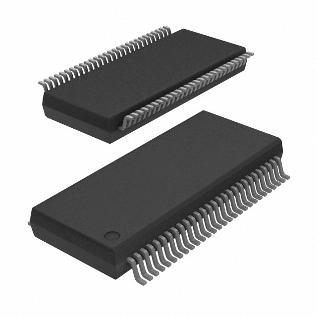
The 74LVCH16601APVG is available in a standard 48-pin TSSOP (Thin Shrink Small Outline Package) package.
Essence
This IC serves as a versatile interface between different digital systems, enabling efficient data transfer and signal conversion.
Packaging/Quantity
The 74LVCH16601APVG is typically sold in reels or tubes containing multiple units. The exact quantity may vary depending on the supplier.
Specifications
- Supply Voltage Range: 2.7V to 3.6V
- Input Voltage Range: 0V to VCC
- Output Voltage Range: 0V to VCC
- Maximum Operating Frequency: 200 MHz
- Number of Inputs/Outputs: 18
Detailed Pin Configuration
The 74LVCH16601APVG has a total of 48 pins, each serving a specific function. Here is a detailed pin configuration:
- A1: Input/Output pin
- B1: Input/Output pin
- Y1: Output pin
- GND: Ground pin
- Y2: Output pin
- B2: Input/Output pin
- A2: Input/Output pin
- VCC: Power supply pin
- A3: Input/Output pin
- B3: Input/Output pin
- Y3: Output pin
- GND: Ground pin
- Y4: Output pin
- B4: Input/Output pin
- A4: Input/Output pin
- VCC: Power supply pin
- A5: Input/Output pin
- B5: Input/Output pin
- Y5: Output pin
- GND: Ground pin
- Y6: Output pin
- B6: Input/Output pin
- A6: Input/Output pin
- VCC: Power supply pin
- A7: Input/Output pin
- B7: Input/Output pin
- Y7: Output pin
- GND: Ground pin
- Y8: Output pin
- B8: Input/Output pin
- A8: Input/Output pin
- VCC: Power supply pin
- A9: Input/Output pin
- B9: Input/Output pin
- Y9: Output pin
- GND: Ground pin
- Y10: Output pin
- B10: Input/Output pin
- A10: Input/Output pin
- VCC: Power supply pin
- A11: Input/Output pin
- B11: Input/Output pin
- Y11: Output pin
- GND: Ground pin
- Y12: Output pin
- B12: Input/Output pin
- A12: Input/Output pin
- VCC: Power supply pin
Functional Features
The 74LVCH16601APVG offers the following functional features:
- Data buffering: It provides bidirectional data buffering, allowing seamless communication between different digital systems.
- Voltage level shifting: This IC can convert signals from one voltage level to another, enabling compatibility between systems operating at different voltages.
- Output enable control: The output pins can be enabled or disabled using the OE (Output Enable) pin, providing flexibility in controlling signal transmission.
Advantages and Disadvantages
Advantages
- Low-voltage operation makes it suitable for modern low-power devices.
- High-speed performance enables efficient data processing.
- Wide operating temperature range ensures reliability in various environments.
- Versatile interface for different digital systems.
Disadvantages
- Limited number of inputs/outputs may restrict its application in complex systems.
- Availability and pricing may vary depending on the supplier.
Working Principles
The 74LVCH16601APVG operates based on CMOS (Complementary Metal-Oxide-Semiconductor) technology. It
قم بإدراج 10 أسئلة وإجابات شائعة تتعلق بتطبيق 74LVCH16601APVG في الحلول التقنية
Sure! Here are 10 common questions and answers related to the application of 74LVCH16601APVG in technical solutions:
Q: What is the function of the 74LVCH16601APVG? A: The 74LVCH16601APVG is a 18-bit universal bus transceiver with 3-state outputs.
Q: What voltage levels does the 74LVCH16601APVG support? A: It supports voltage levels from 1.2V to 3.6V.
Q: Can the 74LVCH16601APVG be used for bidirectional communication? A: Yes, it can be used for bidirectional data flow between two buses.
Q: What is the maximum data transfer rate supported by the 74LVCH16601APVG? A: It supports high-speed operation with a maximum data transfer rate of 400 Mbps.
Q: How many 74LVCH16601APVG devices can be connected together in a system? A: Multiple devices can be connected together to form larger bus widths.
Q: Does the 74LVCH16601APVG have built-in ESD protection? A: Yes, it has built-in ESD protection up to 2000V.
Q: Can the 74LVCH16601APVG operate in a wide temperature range? A: Yes, it can operate in a temperature range of -40°C to +85°C.
Q: What is the power supply voltage range for the 74LVCH16601APVG? A: It has a power supply voltage range of 1.2V to 3.6V.
Q: Does the 74LVCH16601APVG support hot insertion? A: Yes, it supports hot insertion, allowing for easy system maintenance.
Q: Can the 74LVCH16601APVG be used in battery-powered applications? A: Yes, it can be used in battery-powered applications due to its low power consumption.
Please note that these answers are general and may vary depending on the specific application and requirements.