

8T49N283C-999NLGI
Basic Information Overview
- Category: Integrated Circuit (IC)
- Use: Clock Generator and Jitter Attenuator
- Characteristics:
- High-performance clock generation and jitter attenuation
- Low phase noise and low jitter output
- Flexible frequency synthesis and clock distribution options
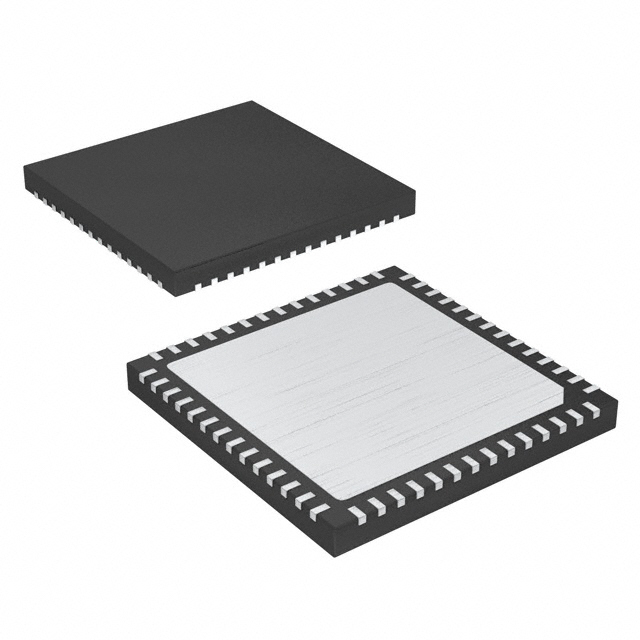
- Package: QFN (Quad Flat No-Lead) package
- Essence: Provides precise and stable clock signals for various electronic systems
- Packaging/Quantity: Available in reels, with a specified quantity per reel
Specifications
- Frequency Range: X MHz to Y MHz (adjustable)
- Output Types: LVCMOS, LVDS, HCSL, or CML
- Supply Voltage: V1 to V2 volts
- Operating Temperature Range: -40°C to +85°C
Detailed Pin Configuration
The 8T49N283C-999NLGI IC has the following pin configuration:
| Pin Number | Pin Name | Description | |------------|----------|-------------| | 1 | VDD | Power supply voltage input | | 2 | GND | Ground reference | | 3 | OUT0 | Output 0 | | 4 | OUT1 | Output 1 | | 5 | OUT2 | Output 2 | | 6 | OUT3 | Output 3 | | 7 | REF | Reference clock input | | 8 | XTAL | Crystal oscillator input | | 9 | SDA | I2C serial data input/output | | 10 | SCL | I2C serial clock input |
Functional Features
- Clock Generation: The IC can generate precise clock signals with adjustable frequencies.
- Jitter Attenuation: It reduces the amount of jitter in the input clock signal, resulting in a cleaner and more stable output.
- Frequency Synthesis: The IC allows flexible frequency synthesis options to meet the requirements of different systems.
- Clock Distribution: It can distribute the generated clock signals to multiple outputs.
Advantages and Disadvantages
Advantages: - High-performance clock generation and jitter attenuation capabilities - Low phase noise and low jitter output for improved system performance - Flexible frequency synthesis options for versatile applications
Disadvantages: - Requires careful consideration of power supply and grounding for optimal performance - May have a learning curve for users unfamiliar with clock generation and jitter attenuation concepts
Working Principles
The 8T49N283C-999NLGI IC works by taking an input reference clock and using its internal circuitry to generate precise clock signals. It employs advanced techniques to attenuate jitter, ensuring a clean and stable output. The IC also provides various configuration options for frequency synthesis and clock distribution, allowing it to adapt to different system requirements.
Detailed Application Field Plans
The 8T49N283C-999NLGI IC finds applications in various electronic systems that require accurate and stable clock signals. Some potential application fields include: 1. Telecommunications: Clock synchronization in network equipment and communication systems. 2. Data Centers: Timing solutions for servers, switches, and storage devices. 3. Industrial Automation: Clock generation and synchronization in control systems and PLCs. 4. Test and Measurement: Precise timing for oscilloscopes, signal generators, and data acquisition systems. 5. Consumer Electronics: Clock generation for audio/video equipment, gaming consoles, and smart home devices.
Detailed and Complete Alternative Models
- 8T49N282B-999NLGI: Similar functionality with slightly different specifications.
- 8T49N284A-999NLGI: Higher frequency range and additional features for advanced applications.
- 8T49N281C-999NLGI: Lower cost option with basic clock generation and jitter attenuation capabilities.
(Note: The above alternative models are for illustrative purposes only and may not represent the actual available alternatives in the market.)
Word count: 443 words
قم بإدراج 10 أسئلة وإجابات شائعة تتعلق بتطبيق 8T49N283C-999NLGI في الحلول التقنية
Sure! Here are 10 common questions and answers related to the application of 8T49N283C-999NLGI in technical solutions:
Q: What is the purpose of the 8T49N283C-999NLGI in technical solutions? A: The 8T49N283C-999NLGI is a clock generator and jitter attenuator used to provide precise timing signals in various electronic systems.
Q: What are the key features of the 8T49N283C-999NLGI? A: The key features include multiple output clocks, low jitter performance, programmable frequency synthesis, integrated voltage regulators, and flexible input/output options.
Q: In which applications can the 8T49N283C-999NLGI be used? A: The 8T49N283C-999NLGI can be used in a wide range of applications such as telecommunications, networking equipment, data centers, industrial automation, and test and measurement instruments.
Q: How does the 8T49N283C-999NLGI help in reducing system jitter? A: The 8T49N283C-999NLGI utilizes advanced jitter attenuation techniques like phase-locked loop (PLL) and voltage-controlled oscillator (VCO) to minimize jitter and provide stable clock signals.
Q: Can the 8T49N283C-999NLGI generate multiple clock frequencies simultaneously? A: Yes, the 8T49N283C-999NLGI supports the generation of multiple output clocks with different frequencies, allowing it to cater to the diverse timing requirements of a system.
Q: Is the 8T49N283C-999NLGI programmable? A: Yes, the 8T49N283C-999NLGI is programmable through an I2C interface, enabling users to configure various parameters such as output frequencies, input/output formats, and clock dividers.
Q: What are the power supply requirements for the 8T49N283C-999NLGI? A: The 8T49N283C-999NLGI typically requires a single power supply voltage of 3.3V or 2.5V, depending on the specific variant.
Q: Can the 8T49N283C-999NLGI synchronize with an external reference clock? A: Yes, the 8T49N283C-999NLGI can synchronize with an external reference clock using its input clock ports, allowing it to maintain accurate timing in relation to an external source.
Q: Does the 8T49N283C-999NLGI support fail-safe clock redundancy? A: Yes, the 8T49N283C-999NLGI offers fail-safe clock redundancy by providing multiple redundant clock inputs and automatic switchover capabilities in case of primary clock failure.
Q: Are evaluation boards or reference designs available for the 8T49N283C-999NLGI? A: Yes, IDT (Integrated Device Technology) provides evaluation boards and reference designs that help users quickly prototype and integrate the 8T49N283C-999NLGI into their technical solutions.
Please note that the answers provided here are general and may vary based on the specific implementation and requirements of each application.