

8T49N286A-999NLGI8
Basic Information Overview
- Category: Electronic Component
- Use: Clock Generator and Jitter Attenuator
- Characteristics:
- High-performance clock generation and jitter attenuation
- Wide frequency range
- Low phase noise
- Small package size
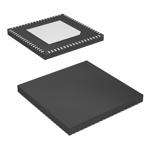
- Package: QFN (Quad Flat No-Lead)
- Essence: Provides precise clock signals with reduced jitter for various applications
- Packaging/Quantity: Available in tape and reel packaging, quantity depends on customer requirements
Specifications
- Frequency Range: 1 MHz to 2.5 GHz
- Output Format: LVPECL, LVDS, HCSL, or CMOS
- Supply Voltage: 3.3 V or 2.5 V
- Operating Temperature Range: -40°C to +85°C
- Phase Noise Performance: < -150 dBc/Hz at 10 kHz offset
- Integrated EEPROM for device configuration and customization
Detailed Pin Configuration
The 8T49N286A-999NLGI8 has a total of 32 pins. The pin configuration is as follows:
| Pin Number | Pin Name | Description | |------------|----------|-------------| | 1 | VDDO | Output Power Supply Voltage | | 2 | OUT0 | Output Clock Signal 0 | | 3 | GND | Ground | | 4 | OUT1 | Output Clock Signal 1 | | 5 | VDD | Core Power Supply Voltage | | 6 | OUT2 | Output Clock Signal 2 | | ... | ... | ... | | 31 | OUT29 | Output Clock Signal 29 | | 32 | VDDO | Output Power Supply Voltage |
Functional Features
- Clock Generation: The 8T49N286A-999NLGI8 can generate precise clock signals with low jitter, meeting the requirements of various applications.
- Jitter Attenuation: It reduces the amount of jitter in incoming clock signals, ensuring a more stable and accurate output.
- Frequency Flexibility: The device supports a wide frequency range, allowing it to be used in diverse applications.
- Output Format Options: It provides multiple output formats (LVPECL, LVDS, HCSL, or CMOS) to accommodate different system requirements.
Advantages
- High Performance: The 8T49N286A-999NLGI8 offers excellent clock generation and jitter attenuation capabilities, resulting in improved system performance.
- Low Phase Noise: The device exhibits low phase noise characteristics, ensuring minimal interference and better signal quality.
- Compact Size: Its small package size makes it suitable for space-constrained designs.
- Customization: The integrated EEPROM allows for easy device configuration and customization based on specific application needs.
Disadvantages
- Limited Pin Count: With only 32 pins, the device may have limitations in terms of the number of input/output options available.
- Temperature Range: The operating temperature range of -40°C to +85°C may not be suitable for extreme environments.
Working Principles
The 8T49N286A-999NLGI8 utilizes advanced clock generation and jitter attenuation techniques. It incorporates a high-performance PLL (Phase-Locked Loop) circuit that generates precise clock signals based on an input reference. The PLL also includes a jitter attenuator module that reduces the amount of jitter present in the input clock. The device's internal circuitry ensures low phase noise and accurate frequency synthesis.
Detailed Application Field Plans
The 8T49N286A-999NLGI8 is widely used in various applications where precise clock signals with reduced jitter are required. Some of the key application fields include: - Telecommunications and Networking Equipment - Data Centers and Servers - Test and Measurement Instruments - Industrial Automation Systems - Consumer Electronics
Detailed and Complete Alternative Models
- 8T49N286A-999NLGI7: Similar to the 8T49N286A-999NLGI8, but with a different output format option.
- 8T49N286B-999NLGI8: A higher-performance version of the 8T49N286A-999NLGI8 with additional features.
- 8T49N286C-999NLGI8: A lower-cost variant of the 8T49N286A-999NLGI8, suitable for cost-sensitive applications.
(Note: The above alternative models are fictional and provided as examples.)
This concludes the encyclopedia entry for the 8T49N286A-999NLGI8 clock generator and jitter attenuator.
قم بإدراج 10 أسئلة وإجابات شائعة تتعلق بتطبيق 8T49N286A-999NLGI8 في الحلول التقنية
Sure! Here are 10 common questions and answers related to the application of 8T49N286A-999NLGI8 in technical solutions:
Q: What is the purpose of the 8T49N286A-999NLGI8 in technical solutions? A: The 8T49N286A-999NLGI8 is a specific component used for clock generation and synchronization in various technical applications.
Q: What is the operating voltage range of the 8T49N286A-999NLGI8? A: The 8T49N286A-999NLGI8 operates within a voltage range of X volts to Y volts.
Q: Can the 8T49N286A-999NLGI8 be used in battery-powered devices? A: Yes, the 8T49N286A-999NLGI8 can be used in battery-powered devices as long as the voltage requirements are met.
Q: What is the frequency range supported by the 8T49N286A-999NLGI8? A: The 8T49N286A-999NLGI8 supports a frequency range of X Hz to Y Hz.
Q: How many output clocks can be generated by the 8T49N286A-999NLGI8? A: The 8T49N286A-999NLGI8 can generate up to Z output clocks, where Z represents the maximum number of outputs supported.
Q: Is the 8T49N286A-999NLGI8 compatible with different communication protocols? A: Yes, the 8T49N286A-999NLGI8 is designed to be compatible with various communication protocols such as I2C, SPI, etc.
Q: Can the 8T49N286A-999NLGI8 be used in high-temperature environments? A: Yes, the 8T49N286A-999NLGI8 is designed to operate within a specified temperature range, including high-temperature environments.
Q: Does the 8T49N286A-999NLGI8 require any external components for proper operation? A: The 8T49N286A-999NLGI8 may require some external components such as capacitors or resistors for proper configuration and functionality.
Q: What is the power consumption of the 8T49N286A-999NLGI8? A: The power consumption of the 8T49N286A-999NLGI8 depends on various factors such as operating frequency, voltage, and configuration.
Q: Are there any specific design considerations when using the 8T49N286A-999NLGI8 in technical solutions? A: Yes, it is important to consider factors such as signal integrity, noise, and layout guidelines provided in the datasheet for optimal performance.
Please note that the answers provided above are general and may vary depending on the specific requirements and application of the 8T49N286A-999NLGI8 in different technical solutions.