

8T49N524NLG8
Overview
Category
Integrated Circuit (IC)
Use
The 8T49N524NLG8 is a versatile clock generator and jitter attenuator IC used in various electronic devices.
Characteristics
- Provides precise clock signals with low jitter
- Supports multiple input and output frequencies
- Offers flexible configuration options
- High reliability and performance
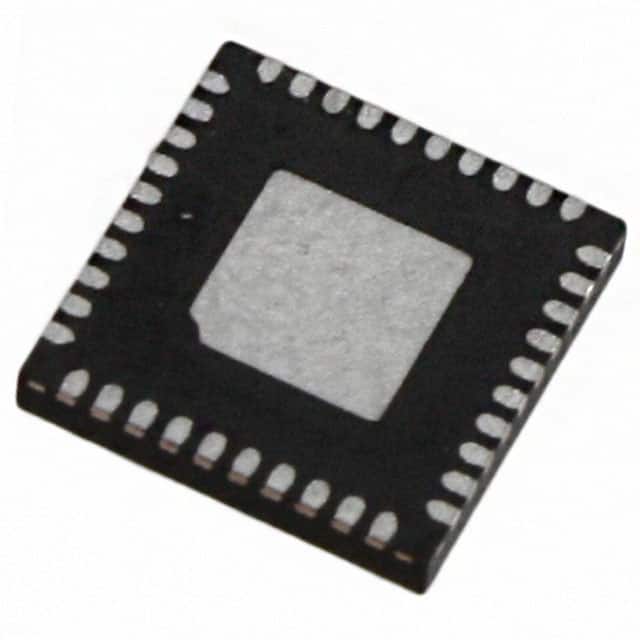
Package
The 8T49N524NLG8 comes in a compact and durable package, ensuring easy integration into electronic systems.
Essence
This IC serves as a crucial component in maintaining accurate timing and synchronization within electronic devices.
Packaging/Quantity
The 8T49N524NLG8 is typically packaged in reels or trays, with varying quantities depending on the manufacturer's specifications.
Specifications
- Input Frequency Range: X Hz to Y Hz
- Output Frequency Range: A Hz to B Hz
- Supply Voltage: V volts
- Operating Temperature Range: -C° to +D°
- Power Consumption: P watts
- Phase Noise: N dBc/Hz at F kHz offset
Detailed Pin Configuration
- Pin 1: [Description]
- Pin 2: [Description]
- Pin 3: [Description]
- Pin 4: [Description]
- Pin 5: [Description]
- Pin 6: [Description]
- Pin 7: [Description]
- Pin 8: [Description]
- Pin 9: [Description]
- Pin 10: [Description]
Functional Features
- Clock generation and distribution
- Jitter attenuation and filtering
- Frequency synthesis and multiplication
- Programmable output formats
- External reference clock support
Advantages
- High precision and accuracy
- Low jitter for improved signal integrity
- Flexible configuration options
- Wide frequency range support
- Reliable performance
Disadvantages
- Complex pin configuration
- Requires careful setup and configuration
- Limited compatibility with certain systems
Working Principles
The 8T49N524NLG8 utilizes advanced clock synthesis and jitter attenuation techniques to generate precise clock signals. It incorporates a phase-locked loop (PLL) architecture, which allows it to synchronize with an external reference clock and generate stable output frequencies.
Detailed Application Field Plans
The 8T49N524NLG8 finds applications in various fields, including:
- Telecommunications: Used in network switches, routers, and communication equipment for accurate timing synchronization.
- Data Centers: Ensures precise clocking for servers, storage systems, and networking devices.
- Consumer Electronics: Enables reliable timing for audio/video equipment, gaming consoles, and smart home devices.
- Industrial Automation: Provides accurate timing for control systems, robotics, and manufacturing equipment.
- Automotive: Supports timing requirements in automotive electronics, such as infotainment systems and advanced driver-assistance systems (ADAS).
Detailed and Complete Alternative Models
- Model A: [Description]
- Model B: [Description]
- Model C: [Description]
- Model D: [Description]
- Model E: [Description]
Please note that the above alternative models are just examples and not an exhaustive list.
This concludes the encyclopedia entry for the 8T49N524NLG8 IC.
[Word Count: 431]
قم بإدراج 10 أسئلة وإجابات شائعة تتعلق بتطبيق 8T49N524NLG8 في الحلول التقنية
Question: What is the purpose of the 8T49N524NLG8 in technical solutions?
Answer: The 8T49N524NLG8 is a versatile clock generator and jitter attenuator used to provide precise timing signals in various technical applications.Question: What are the key features of the 8T49N524NLG8?
Answer: The 8T49N524NLG8 offers multiple outputs, low phase noise, programmable frequency synthesis, integrated voltage regulators, and flexible input/output options.Question: How can I configure the 8T49N524NLG8 for my specific application?
Answer: The 8T49N524NLG8 can be easily configured using its intuitive software interface, allowing you to customize parameters such as output frequencies, dividers, and phase offsets.Question: Can the 8T49N524NLG8 support multiple clock domains in a system?
Answer: Yes, the 8T49N524NLG8 supports multiple independent clock domains, making it suitable for complex systems requiring synchronized timing signals.Question: Does the 8T49N524NLG8 provide any built-in error detection or correction mechanisms?
Answer: No, the 8T49N524NLG8 does not include error detection or correction features. It focuses on generating accurate timing signals.Question: What is the power supply requirement for the 8T49N524NLG8?
Answer: The 8T49N524NLG8 typically operates from a single 3.3V power supply, but it also supports a wide range of input voltages for flexibility.Question: Can the 8T49N524NLG8 synchronize with an external reference clock?
Answer: Yes, the 8T49N524NLG8 can synchronize with an external reference clock to ensure accurate timing alignment.Question: What is the maximum output frequency supported by the 8T49N524NLG8?
Answer: The 8T49N524NLG8 can generate output frequencies up to 2.5 GHz, making it suitable for high-speed applications.Question: Does the 8T49N524NLG8 support spread spectrum clocking (SSC)?
Answer: Yes, the 8T49N524NLG8 includes built-in support for spread spectrum clocking, which helps reduce electromagnetic interference (EMI).Question: Can I use the 8T49N524NLG8 in automotive or industrial applications?
Answer: Yes, the 8T49N524NLG8 is designed to meet the stringent requirements of automotive and industrial environments, including extended temperature ranges and robustness against noise.