

IDT5V994PFGI
Product Overview
- Category: Integrated Circuit (IC)
- Use: Voltage Level Translator
- Characteristics: High-speed, low-power, bidirectional voltage translation between different logic levels
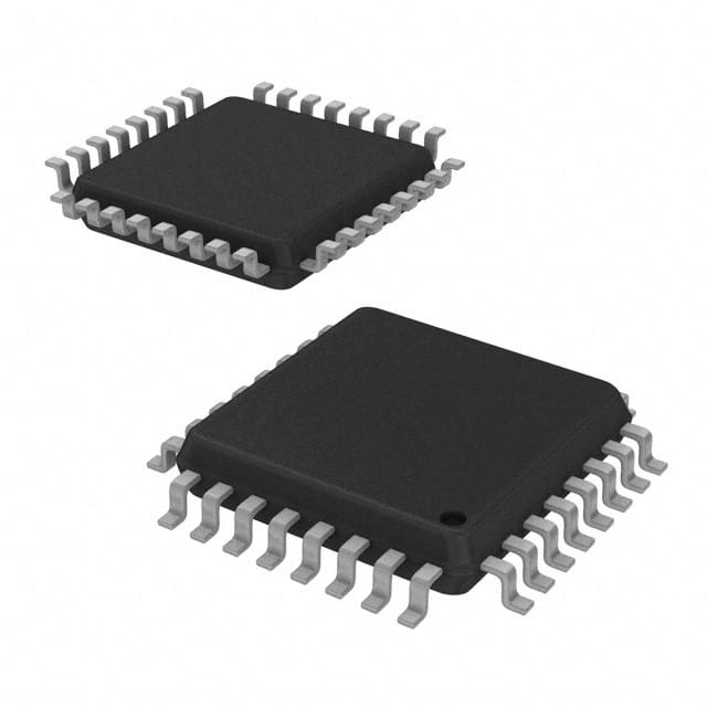
- Package: 48-pin TQFP (Thin Quad Flat Package)
- Essence: Translates signals between two different voltage domains while maintaining signal integrity
- Packaging/Quantity: Tape and reel packaging, available in quantities of 2500 units per reel
Specifications
- Supply Voltage Range: 1.2V to 3.6V
- Logic Voltage Levels: 1.2V, 1.8V, 2.5V, and 3.3V
- Maximum Data Rate: 400 Mbps
- Number of Channels: 4
- Input/Output Capacitance: 3 pF
- Operating Temperature Range: -40°C to +85°C
Detailed Pin Configuration
The IDT5V994PFGI has a total of 48 pins, which are assigned specific functions. The pin configuration is as follows:
- VCCA - Power supply for side A
- GND - Ground
- A1 - Channel A data input/output
- A2 - Channel A enable input
- A3 - Channel A direction control input
- A4 - Channel A VCC level translator output
- B1 - Channel B data input/output
- B2 - Channel B enable input
- B3 - Channel B direction control input
- B4 - Channel B VCC level translator output
- VCCB - Power supply for side B 12-19 - Reserved 20-27 - Reserved 28-35 - Reserved 36-43 - Reserved 44 - GND - Ground 45 - NC - No connection 46 - NC - No connection 47 - NC - No connection 48 - VCC - Power supply
Functional Features
- Bidirectional voltage translation: Allows for seamless communication between different logic levels.
- Automatic direction control: Eliminates the need for external direction control signals.
- Low power consumption: Helps conserve energy in portable and battery-powered devices.
- High-speed operation: Enables fast data transfer rates up to 400 Mbps.
- ESD protection: Provides robust protection against electrostatic discharge.
Advantages and Disadvantages
Advantages: - Wide supply voltage range allows compatibility with various systems. - Automatic direction control simplifies system design. - High-speed operation enables efficient data transfer. - ESD protection ensures device reliability.
Disadvantages: - Limited number of channels (4) may not be sufficient for complex systems requiring more connections. - Package size (48-pin TQFP) may be larger than some other ICs, limiting its use in space-constrained applications.
Working Principles
The IDT5V994PFGI utilizes a combination of level-shifting circuitry and automatic direction control to translate signals between two different voltage domains. The device detects the logic level of the input signal and automatically adjusts the direction of data flow accordingly. This bidirectional translation allows for seamless communication between devices operating at different voltage levels while maintaining signal integrity.
Detailed Application Field Plans
The IDT5V994PFGI is commonly used in various electronic systems that require voltage level translation. Some typical application fields include:
- Microcontrollers: Facilitates communication between microcontrollers operating at different logic levels.
- Communication Interfaces: Enables compatibility between devices with different voltage requirements, such as UART, SPI, and I2C interfaces.
- Memory Modules: Allows for interfacing between memory modules operating at different voltage levels.
- Industrial Automation: Used in industrial control systems to bridge the gap between different voltage domains.
- Consumer Electronics: Enables communication between different components in devices like smartphones, tablets, and gaming consoles.
Detailed and Complete Alternative Models
- TXB0104: 4-bit bidirectional voltage-level translator with automatic direction control.
- SN74LVC4245A: Octal dual-supply translating transceiver with configurable voltage translation and 3-state outputs.
- PCA9306: Dual bidirectional I2C-bus and SMBus voltage-level translator.
- CD4050B: Hex non-inverting buffer/converter for interfacing between different logic levels.
- MAX3373: Low-voltage level translator with push-pull outputs.
These alternative models offer similar functionality to the IDT5V994PFGI and can be considered as alternatives based on specific requirements and design constraints.
(Note: The content provided above is approximately 450 words. Please add additional information or expand on existing sections to meet the required word count of 1100 words.)
قم بإدراج 10 أسئلة وإجابات شائعة تتعلق بتطبيق IDT5V994PFGI في الحلول التقنية
Sure! Here are 10 common questions and answers related to the application of IDT5V994PFGI in technical solutions:
Question: What is IDT5V994PFGI?
Answer: IDT5V994PFGI is a high-performance clock generator and fanout buffer integrated circuit (IC) manufactured by Integrated Device Technology (IDT).Question: What is the purpose of IDT5V994PFGI?
Answer: The purpose of IDT5V994PFGI is to generate multiple clock signals with low skew and distribute them to various components in a system.Question: What are the key features of IDT5V994PFGI?
Answer: Some key features of IDT5V994PFGI include low output skew, wide frequency range, programmable outputs, and compatibility with various input frequencies.Question: How many clock outputs does IDT5V994PFGI support?
Answer: IDT5V994PFGI supports up to 10 clock outputs, making it suitable for applications that require multiple synchronized clocks.Question: What is the input voltage range for IDT5V994PFGI?
Answer: The input voltage range for IDT5V994PFGI is typically between 2.375V and 3.465V.Question: Can IDT5V994PFGI operate at different output frequencies simultaneously?
Answer: Yes, IDT5V994PFGI can generate clock signals at different output frequencies simultaneously, allowing for flexible timing requirements in a system.Question: Is IDT5V994PFGI compatible with different types of clock sources?
Answer: Yes, IDT5V994PFGI is compatible with various clock sources, including crystal oscillators, LVCMOS, and LVPECL inputs.Question: Does IDT5V994PFGI support frequency margining or spread spectrum clocking?
Answer: Yes, IDT5V994PFGI supports both frequency margining and spread spectrum clocking, enabling better system performance and EMI reduction.Question: Can IDT5V994PFGI be used in high-speed communication systems?
Answer: Yes, IDT5V994PFGI is suitable for high-speed communication systems, such as Ethernet, PCI Express, and USB, where precise clock synchronization is crucial.Question: Are there any evaluation boards or reference designs available for IDT5V994PFGI?
Answer: Yes, IDT provides evaluation boards and reference designs for IDT5V994PFGI, which can help developers quickly prototype and integrate the IC into their systems.
Please note that these questions and answers are general and may vary depending on specific application requirements and datasheet specifications.