

IDT74FCT16500CTPVG8
Product Overview
- Category: Integrated Circuit
- Use: Data Buffer/Line Driver
- Characteristics: High-speed, low-power, 16-bit wide, non-inverting, tri-state buffer/line driver
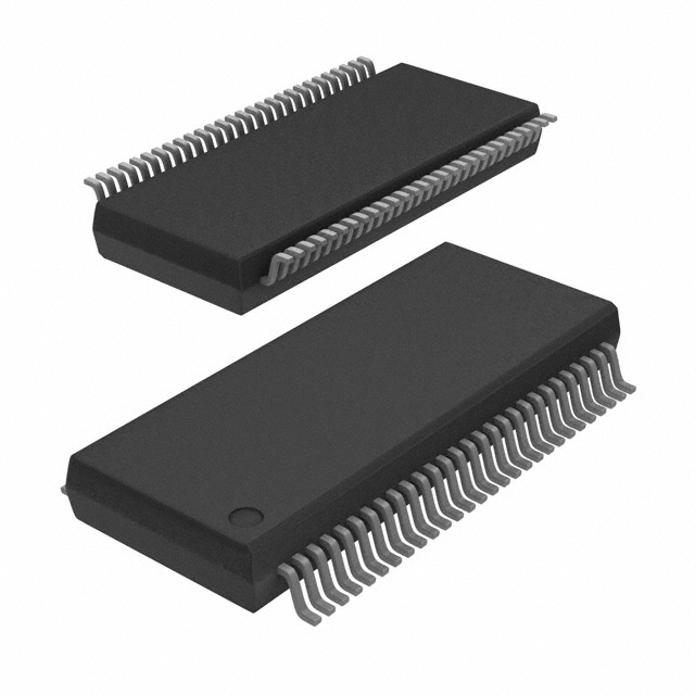
- Package: TSSOP (Thin Shrink Small Outline Package)
- Essence: The IDT74FCT16500CTPVG8 is a high-performance data buffer/line driver designed for use in various digital systems.
- Packaging/Quantity: Available in tape and reel packaging with 2500 units per reel.
Specifications
- Number of Bits: 16
- Logic Family: FCT
- Input Voltage: 4.5V to 5.5V
- Output Voltage: 4.5V to 5.5V
- Operating Temperature Range: -40°C to +85°C
- Propagation Delay Time: 3.5ns (typical)
- Output Current: ±24mA
- Supply Current: 50mA (max)
Detailed Pin Configuration
The IDT74FCT16500CTPVG8 has a 48-pin TSSOP package with the following pin configuration:
- OE (Output Enable) 1
- Y0 (Output) 1
- GND (Ground)
- Y1 (Output) 1
- Y2 (Output) 1
- Y3 (Output) 1
- VCC (Power Supply)
- Y4 (Output) 1
- Y5 (Output) 1
- Y6 (Output) 1
- Y7 (Output) 1
- Y8 (Output) 1
- Y9 (Output) 1
- Y10 (Output) 1
- Y11 (Output) 1
- Y12 (Output) 1
- Y13 (Output) 1
- Y14 (Output) 1
- Y15 (Output) 1
- GND (Ground)
- OE (Output Enable) 2
- Y0 (Output) 2
- GND (Ground)
- Y1 (Output) 2
- Y2 (Output) 2
- Y3 (Output) 2
- VCC (Power Supply)
- Y4 (Output) 2
- Y5 (Output) 2
- Y6 (Output) 2
- Y7 (Output) 2
- Y8 (Output) 2
- Y9 (Output) 2
- Y10 (Output) 2
- Y11 (Output) 2
- Y12 (Output) 2
- Y13 (Output) 2
- Y14 (Output) 2
- Y15 (Output) 2
- GND (Ground)
Functional Features
- Non-inverting buffer/line driver: The IDT74FCT16500CTPVG8 provides non-inverting functionality, ensuring that the output signal matches the input signal.
- Tri-state outputs: The device features tri-state outputs, allowing multiple devices to be connected to a common bus without interference.
- High-speed operation: With a propagation delay time of 3.5ns, the IDT74FCT16500CTPVG8 is capable of handling high-speed data transmission.
- Low power consumption: The integrated circuit is designed to operate with low power consumption, making it suitable for battery-powered applications.
Advantages and Disadvantages
Advantages: - High-speed operation enables efficient data transfer. - Tri-state outputs allow for easy bus sharing. - Low power consumption extends battery life in portable devices.
Disadvantages: - Limited voltage range (4.5V to 5.5V) may not be suitable for all applications. - The TSSOP package may require careful handling during assembly.
Working Principles
The IDT74FCT16500CTPVG8 functions as a buffer/line driver by amplifying and transmitting digital signals. When the output enable (OE) pin is active, the input signal is amplified and passed through to the corresponding output pins. When the OE pin is inactive, the outputs are in a high-impedance state, allowing other devices to drive the bus.
Detailed Application Field Plans
The IDT74FCT16500CTPVG8 is commonly used in various digital systems, including:
- Microprocessors and microcontrollers
- Memory modules
- Communication systems
- Industrial automation equipment
- Test and measurement instruments
Detailed and Complete Alternative Models
- SN74FCT
قم بإدراج 10 أسئلة وإجابات شائعة تتعلق بتطبيق IDT74FCT16500CTPVG8 في الحلول التقنية
Sure! Here are 10 common questions and answers related to the application of IDT74FCT16500CTPVG8 in technical solutions:
Q: What is the IDT74FCT16500CTPVG8? A: The IDT74FCT16500CTPVG8 is a 16-bit universal bus transceiver with 3-state outputs.
Q: What is the purpose of the IDT74FCT16500CTPVG8? A: It is used for bidirectional data communication between two buses or systems.
Q: What voltage levels does the IDT74FCT16500CTPVG8 support? A: It supports both TTL (Transistor-Transistor Logic) and CMOS (Complementary Metal-Oxide-Semiconductor) voltage levels.
Q: What is the maximum operating frequency of the IDT74FCT16500CTPVG8? A: The maximum operating frequency is typically around 100 MHz.
Q: How many data lines can the IDT74FCT16500CTPVG8 handle? A: It can handle up to 16 data lines.
Q: Can the IDT74FCT16500CTPVG8 be used as a level shifter? A: Yes, it can be used to convert signals between different voltage levels.
Q: Does the IDT74FCT16500CTPVG8 have any built-in protection features? A: Yes, it has built-in ESD (Electrostatic Discharge) protection on all inputs and outputs.
Q: What is the power supply voltage range for the IDT74FCT16500CTPVG8? A: The power supply voltage range is typically between 4.5V and 5.5V.
Q: Can the IDT74FCT16500CTPVG8 be used in high-speed data transmission applications? A: Yes, it can be used in applications that require high-speed data transmission.
Q: Are there any specific application notes or reference designs available for the IDT74FCT16500CTPVG8? A: Yes, the datasheet of the IDT74FCT16500CTPVG8 provides detailed application notes and reference designs for various use cases.
Please note that these answers are general and may vary depending on the specific requirements and implementation of the IDT74FCT16500CTPVG8 in a technical solution.