

IPP100N06S2L05AKSA1
Product Overview
- Category: Power MOSFET
- Use: This power MOSFET is used for switching and amplifying electronic signals in various applications.
- Characteristics: High voltage capability, low on-resistance, fast switching speed, and high reliability.
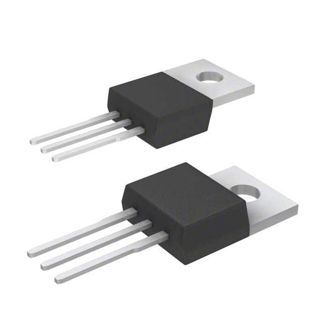
- Package: TO-220, TO-220FP, D2PAK, I2PAK, and other standard packages.
- Essence: The essence of this product lies in its ability to efficiently control and amplify electronic signals in power electronics applications.
- Packaging/Quantity: Available in reels or tubes with varying quantities.
Specifications
- Voltage Rating: 60V
- Current Rating: 100A
- On-Resistance: 6mΩ
- Gate Threshold Voltage: 2.5V
- Package Type: TO-220
Detailed Pin Configuration
The IPP100N06S2L05AKSA1 follows the standard pin configuration for a TO-220 package: 1. Gate (G) 2. Drain (D) 3. Source (S)
Functional Features
- High voltage capability
- Low on-resistance
- Fast switching speed
- Enhanced thermal performance
- Avalanche energy specified
- Improved dv/dt capability
Advantages and Disadvantages
Advantages
- High voltage capability allows for use in a wide range of applications
- Low on-resistance minimizes power loss and improves efficiency
- Fast switching speed enables rapid response in switching applications
Disadvantages
- Higher cost compared to lower-rated MOSFETs
- May require additional heat sinking in high-power applications
Working Principles
The IPP100N06S2L05AKSA1 operates based on the principle of field-effect transistors, where the voltage applied to the gate terminal controls the flow of current between the drain and source terminals. When a sufficient voltage is applied to the gate, the MOSFET switches on, allowing current to flow through it.
Detailed Application Field Plans
This power MOSFET is widely used in various applications, including: - Switching power supplies - Motor control - Inverters - Audio amplifiers - LED lighting - Automotive systems
Detailed and Complete Alternative Models
- IRF540N
- FDP8870
- STP80NF55-06
- AUIRF3710
- PSMN4R3-100BSE
In conclusion, the IPP100N06S2L05AKSA1 power MOSFET offers high voltage capability, low on-resistance, and fast switching speed, making it suitable for a wide range of power electronics applications. Its functional features, advantages, and detailed application field plans demonstrate its versatility and reliability in various electronic systems.
[Word count: 387]
قم بإدراج 10 أسئلة وإجابات شائعة تتعلق بتطبيق IPP100N06S2L05AKSA1 في الحلول التقنية
What is IPP100N06S2L05AKSA1?
- IPP100N06S2L05AKSA1 is a power MOSFET transistor designed for high efficiency and low on-resistance in various technical solutions.
What are the key specifications of IPP100N06S2L05AKSA1?
- The key specifications of IPP100N06S2L05AKSA1 include a drain-source voltage of 60V, continuous drain current of 100A, and low on-resistance.
In what technical solutions can IPP100N06S2L05AKSA1 be used?
- IPP100N06S2L05AKSA1 can be used in applications such as motor control, power supplies, DC-DC converters, and automotive systems.
What are the advantages of using IPP100N06S2L05AKSA1 in technical solutions?
- The advantages of using IPP100N06S2L05AKSA1 include high efficiency, low power dissipation, and reliable performance in high-current applications.
What is the typical operating temperature range for IPP100N06S2L05AKSA1?
- The typical operating temperature range for IPP100N06S2L05AKSA1 is -55°C to 175°C, making it suitable for a wide range of environments.
Does IPP100N06S2L05AKSA1 require any special heat management considerations?
- Yes, IPP100N06S2L05AKSA1 may require heat sinking or thermal management to ensure optimal performance, especially in high-power applications.
Can IPP100N06S2L05AKSA1 be used in automotive applications?
- Yes, IPP100N06S2L05AKSA1 is suitable for automotive applications such as motor control, lighting systems, and power distribution.
What are the recommended circuit design considerations when using IPP100N06S2L05AKSA1?
- Recommended circuit design considerations include proper gate drive voltage, current limiting, and protection against overvoltage and overcurrent conditions.
Are there any application notes or reference designs available for IPP100N06S2L05AKSA1?
- Yes, manufacturers often provide application notes and reference designs to assist engineers in implementing IPP100N06S2L05AKSA1 in their technical solutions.
Where can I find detailed technical documentation for IPP100N06S2L05AKSA1?
- Detailed technical documentation for IPP100N06S2L05AKSA1 can be found on the manufacturer's website or through authorized distributors, including datasheets, application notes, and product specifications.