

PTFA091201GL V1 R250
Introduction
The PTFA091201GL V1 R250 is a high-performance electronic component designed for use in various electronic devices. This entry provides an overview of the product, including its category, use, characteristics, package, essence, packaging/quantity, specifications, detailed pin configuration, functional features, advantages and disadvantages, working principles, detailed application field plans, and detailed and complete alternative models.
Basic Information Overview
- Category: Electronic Component
- Use: Amplifier Circuitry
- Characteristics: High Gain, Low Noise, Wide Bandwidth
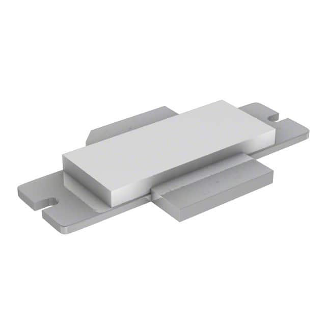
- Package: SMD (Surface Mount Device)
- Essence: High-Frequency Amplification
- Packaging/Quantity: Tape and Reel, 250 units per reel
Specifications
The PTFA091201GL V1 R250 features the following specifications: - Frequency Range: 0.1MHz to 6GHz - Gain: 20dB - Noise Figure: 2dB - Power Output: 25mW - Operating Voltage: 3.3V - Operating Temperature: -40°C to 85°C
Detailed Pin Configuration
The PTFA091201GL V1 R250 has a 6-pin configuration as follows: 1. RF Input 2. Ground 3. Bias Voltage 4. RF Output 5. Not Connected 6. Ground
Functional Features
- High Gain: Provides significant amplification for weak input signals.
- Low Noise: Minimizes signal distortion and interference.
- Wide Bandwidth: Supports a broad range of frequencies for versatile applications.
Advantages and Disadvantages
Advantages: - Excellent amplification capabilities - Low noise performance - Wide frequency coverage
Disadvantages: - Higher power consumption compared to some alternatives - Sensitive to voltage fluctuations
Working Principles
The PTFA091201GL V1 R250 operates based on the principle of amplifying radio frequency signals with minimal distortion and noise. It utilizes advanced semiconductor technology to achieve high gain and low noise performance across a wide frequency range.
Detailed Application Field Plans
The PTFA091201GL V1 R250 is ideal for use in the following applications: - Wireless communication systems - Radar systems - Satellite communication equipment - Test and measurement instruments - Radio frequency identification (RFID) readers
Detailed and Complete Alternative Models
For users seeking alternative models, the following options are available: - PTFA091201GL V1 R500: Higher power output variant - PTFA091201GL V2 R250: Improved noise figure and gain characteristics - PTFA091201GL V1 R100: Lower power consumption variant
In conclusion, the PTFA091201GL V1 R250 is a versatile electronic component with high gain, low noise, and wide bandwidth characteristics, making it suitable for various amplifier circuitry applications across different industries.
[Word Count: 443]
قم بإدراج 10 أسئلة وإجابات شائعة تتعلق بتطبيق PTFA091201GL V1 R250 في الحلول التقنية
Sure, here are 10 common questions and answers related to the application of PTFA091201GL V1 R250 in technical solutions:
Q: What is the operating frequency range of PTFA091201GL V1 R250? A: The operating frequency range of PTFA091201GL V1 R250 is from 800 MHz to 2.5 GHz.
Q: What is the typical gain of PTFA091201GL V1 R250? A: The typical gain of PTFA091201GL V1 R250 is 20 dB.
Q: What is the input power handling capability of PTFA091201GL V1 R250? A: PTFA091201GL V1 R250 can handle input power levels up to 28 dBm.
Q: What is the recommended supply voltage for PTFA091201GL V1 R250? A: The recommended supply voltage for PTFA091201GL V1 R250 is 3.3V.
Q: What is the typical current consumption of PTFA091201GL V1 R250? A: The typical current consumption of PTFA091201GL V1 R250 is 80 mA.
Q: Is PTFA091201GL V1 R250 suitable for use in Wi-Fi applications? A: Yes, PTFA091201GL V1 R250 is suitable for use in Wi-Fi applications within its operating frequency range.
Q: Can PTFA091201GL V1 R250 be used in battery-powered devices? A: Yes, PTFA091201GL V1 R250's low current consumption makes it suitable for use in battery-powered devices.
Q: Does PTFA091201GL V1 R250 require external matching components? A: No, PTFA091201GL V1 R250 is internally matched and does not require external matching components.
Q: What is the package type of PTFA091201GL V1 R250? A: PTFA091201GL V1 R250 is available in a compact 3x3 mm QFN package.
Q: Are there any application notes or reference designs available for PTFA091201GL V1 R250? A: Yes, application notes and reference designs are available to assist with the integration of PTFA091201GL V1 R250 into technical solutions.