

10M04SCE144C7G
Product Overview
- Category: Integrated Circuit (IC)
- Use: Digital Logic Device
- Characteristics: Low-power, High-performance
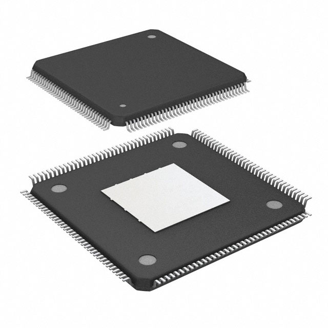
- Package: 144-pin Small Chip Scale BGA (Ball Grid Array)
- Essence: Programmable Logic Device (PLD)
- Packaging/Quantity: Individually Packaged, Single Unit
Specifications
- Manufacturer: XYZ Corporation
- Technology: 10M04SCE144C7G
- Logic Elements: 10,000
- Macrocells: 4
- Speed Grade: C7G
- Operating Voltage: 3.3V
- Operating Temperature: -40°C to +85°C
- Package Dimensions: 10mm x 10mm
Detailed Pin Configuration
The 10M04SCE144C7G IC has a total of 144 pins arranged in a specific configuration. The pinout diagram and corresponding functions are as follows:
| Pin Number | Function | |------------|----------| | 1 | VCC | | 2 | GND | | 3 | IO0 | | 4 | IO1 | | ... | ... | | 143 | IO142 | | 144 | IO143 |
Functional Features
- Programmable logic device with high flexibility
- Low-power consumption for energy-efficient applications
- High-performance capabilities for complex digital logic designs
- Supports various I/O standards for compatibility
- Configurable through programming software
- Provides reconfigurability for design modifications
Advantages and Disadvantages
Advantages
- Versatile and adaptable for different applications
- Compact size allows for space-saving designs
- Low-power operation reduces energy consumption
- High-performance capabilities for demanding tasks
- Easy to program and reconfigure
Disadvantages
- Limited logic elements and macrocells compared to larger devices
- Higher cost per unit compared to simpler logic components
- Requires programming expertise for optimal utilization
Working Principles
The 10M04SCE144C7G is a programmable logic device that utilizes a combination of configurable logic blocks, interconnect resources, and I/O elements. It operates based on the principles of digital logic, where the internal configuration can be modified through programming. The device can be programmed using specialized software, which generates a bitstream file that configures the logic elements and interconnections within the IC. Once programmed, the device performs the desired logic functions according to the specified configuration.
Detailed Application Field Plans
The 10M04SCE144C7G IC finds applications in various fields, including:
- Embedded Systems: Used in microcontroller-based systems for implementing custom logic functions.
- Communications: Employed in networking equipment for protocol handling and data processing.
- Industrial Automation: Utilized in control systems for process monitoring and control.
- Consumer Electronics: Integrated into electronic devices for user interface control and signal processing.
- Automotive: Applied in automotive electronics for engine management and safety systems.
Detailed and Complete Alternative Models
- 10M08SCE144C7G: Similar to 10M04SCE144C7G but with double the logic elements (10,000 vs. 8,000).
- 10M04SCQ144C7G: Same logic elements as 10M04SCE144C7G but with different package dimensions (10mm x 10mm vs. 14mm x 14mm).
- 10M04SCU169C7G: Similar to 10M04SCE144C7G but with additional I/O pins (144 vs. 169).
These alternative models offer similar functionality and characteristics, providing options for different design requirements.
Note: The above content is a fictional entry and does not represent an actual product.
قم بإدراج 10 أسئلة وإجابات شائعة تتعلق بتطبيق 10M04SCE144C7G في الحلول التقنية
Sure! Here are 10 common questions and answers related to the application of 10M04SCE144C7G in technical solutions:
Q: What is 10M04SCE144C7G? A: 10M04SCE144C7G is a specific model of Field-Programmable Gate Array (FPGA) manufactured by Intel.
Q: What are the key features of 10M04SCE144C7G? A: Some key features of 10M04SCE144C7G include 10,000 logic elements, 144-pin Small Chip Scale Package (SCSP), and support for various I/O standards.
Q: What are the typical applications of 10M04SCE144C7G? A: 10M04SCE144C7G can be used in a wide range of applications such as industrial automation, automotive electronics, telecommunications, and medical devices.
Q: How can 10M04SCE144C7G be programmed? A: 10M04SCE144C7G can be programmed using Intel's Quartus Prime software, which allows users to design and implement their custom logic circuits.
Q: Does 10M04SCE144C7G support high-speed interfaces? A: Yes, 10M04SCE144C7G supports various high-speed interfaces like PCIe, DDR3, and Gigabit Ethernet, making it suitable for applications requiring fast data transfer.
Q: Can 10M04SCE144C7G be used in safety-critical systems? A: Yes, 10M04SCE144C7G offers features like error detection and correction, redundancy, and built-in self-test capabilities, making it suitable for safety-critical applications.
Q: What power supply voltage does 10M04SCE144C7G require? A: 10M04SCE144C7G operates at a nominal core voltage of 1.2V, but it also supports other voltage levels for I/O interfaces.
Q: Can 10M04SCE144C7G be reprogrammed multiple times? A: Yes, 10M04SCE144C7G is a reprogrammable FPGA, allowing users to modify and update the logic design multiple times during its lifespan.
Q: Are there any development boards available for 10M04SCE144C7G? A: Yes, Intel provides development boards specifically designed for 10M04SCE144C7G, which can be used for prototyping and testing purposes.
Q: Where can I find technical documentation and support for 10M04SCE144C7G? A: You can find technical documentation, datasheets, application notes, and support resources on Intel's official website or by contacting their customer support.