

10M08SCE144C7G
Product Overview
- Category: Integrated Circuit (IC)
- Use: Digital Logic Device
- Characteristics: Low-power, High-performance, Programmable
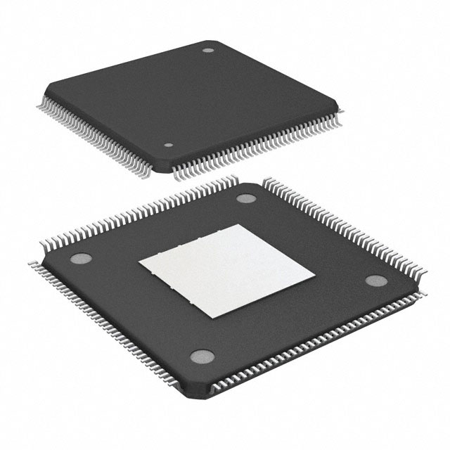
- Package: 144-pin Small Chip Scale BGA (Ball Grid Array)
- Essence: Field-Programmable Gate Array (FPGA)
- Packaging/Quantity: Individually Packaged, Single Unit
Specifications
- Manufacturer: Intel Corporation
- Technology: 10nm
- Logic Elements: 8,000
- Embedded Memory: 1.6 Mb
- Operating Voltage: 1.2V
- Operating Temperature: -40°C to +100°C
- Speed Grade: C7G
Detailed Pin Configuration
The 10M08SCE144C7G has a total of 144 pins arranged in a specific configuration. The pinout diagram and detailed pin descriptions can be found in the product datasheet provided by the manufacturer.
Functional Features
- Programmability: The FPGA can be configured and reconfigured to perform various digital logic functions.
- High Performance: The device offers fast processing speeds and low latency.
- Low Power Consumption: Designed for energy efficiency, it minimizes power consumption during operation.
- Versatility: Supports a wide range of applications due to its programmable nature.
- Integration: Combines multiple logic elements and embedded memory on a single chip.
Advantages and Disadvantages
Advantages: - Flexibility: Can be customized for specific applications. - Time-to-Market: Allows rapid prototyping and development cycles. - Cost-Effective: Eliminates the need for custom ASICs (Application-Specific Integrated Circuits). - Scalability: Can be easily upgraded or modified without hardware changes.
Disadvantages: - Complexity: Requires expertise in FPGA programming and design. - Limited Resources: The number of logic elements and memory is finite. - Power Consumption: Can be higher compared to dedicated hardware solutions for specific tasks.
Working Principles
The 10M08SCE144C7G FPGA operates based on the principles of reconfigurable digital logic. It consists of an array of programmable logic elements interconnected through configurable routing resources. These logic elements can be programmed to implement various digital functions, such as arithmetic operations, data processing, and control logic. The configuration of the FPGA is stored in non-volatile memory and can be modified as needed.
Detailed Application Field Plans
The 10M08SCE144C7G FPGA finds applications in various fields, including:
- Communications: Used in wireless base stations, network routers, and switches for signal processing and protocol handling.
- Industrial Automation: Employed in control systems, robotics, and machine vision applications for real-time data processing and control.
- Medical Devices: Utilized in medical imaging equipment, patient monitoring systems, and laboratory instruments for data acquisition and processing.
- Automotive: Integrated into advanced driver-assistance systems (ADAS), infotainment systems, and engine control units (ECUs) for enhanced functionality.
- Aerospace and Defense: Deployed in radar systems, avionics, and military communication systems for high-performance signal processing and encryption.
Detailed and Complete Alternative Models
- Intel 10M16SAU169C8G
- Xilinx XC7A35T-1CPG236C
- Lattice iCE40UP5K-SG48I
- Microchip ATSAM4LC4CA-AU
- Altera MAX 10M04DCM36C8G
These alternative models offer similar functionality and can be considered as alternatives to the 10M08SCE144C7G FPGA.
Note: The content provided above is a sample structure for an encyclopedia entry. The actual content may vary based on specific product details and requirements.
قم بإدراج 10 أسئلة وإجابات شائعة تتعلق بتطبيق 10M08SCE144C7G في الحلول التقنية
Sure! Here are 10 common questions and answers related to the application of 10M08SCE144C7G in technical solutions:
Q: What is 10M08SCE144C7G? A: 10M08SCE144C7G is a specific model number for an FPGA (Field-Programmable Gate Array) manufactured by Intel.
Q: What are the key features of 10M08SCE144C7G? A: Some key features of 10M08SCE144C7G include 10,000 logic elements, 144-pin package, and support for various I/O standards.
Q: In what applications can 10M08SCE144C7G be used? A: 10M08SCE144C7G can be used in a wide range of applications such as industrial automation, automotive systems, telecommunications, and medical devices.
Q: How can I program 10M08SCE144C7G? A: 10M08SCE144C7G can be programmed using Intel's Quartus Prime software, which allows you to design and implement your digital logic circuits.
Q: What are the power requirements for 10M08SCE144C7G? A: The power requirements for 10M08SCE144C7G typically include a supply voltage of 1.2V and various power rails for different components.
Q: Can 10M08SCE144C7G interface with other devices? A: Yes, 10M08SCE144C7G supports various communication protocols such as SPI, I2C, UART, and Ethernet, allowing it to interface with other devices.
Q: What is the maximum operating frequency of 10M08SCE144C7G? A: The maximum operating frequency of 10M08SCE144C7G depends on the design and implementation, but it can typically reach several hundred megahertz.
Q: Can 10M08SCE144C7G be reprogrammed after deployment? A: Yes, 10M08SCE144C7G is a field-programmable device, which means it can be reprogrammed even after it has been deployed in a system.
Q: Are there any development boards available for 10M08SCE144C7G? A: Yes, Intel provides development boards specifically designed for 10M08SCE144C7G, which can help with prototyping and testing.
Q: Where can I find more information about 10M08SCE144C7G? A: You can find more detailed information about 10M08SCE144C7G, including datasheets and application notes, on Intel's official website or by contacting their support team.
Please note that the specific details and answers may vary depending on the manufacturer and the context of the application.