

10M08SFE144C7G
Product Overview
- Category: Integrated Circuit (IC)
- Use: Digital Logic Device
- Characteristics: High-performance, Low-power consumption
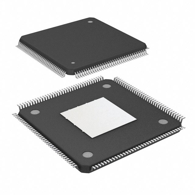
- Package: 144-pin Fine-pitch Ball Grid Array (FBGA)
- Essence: Programmable Logic Device (PLD)
- Packaging/Quantity: Tray packaging, available in bulk quantities
Specifications
- Manufacturer: Intel Corporation
- Family: MAX® 10
- Series: MAX 10M08S
- Device Type: Field-Programmable Gate Array (FPGA)
- Number of Logic Elements: 8,000
- Number of I/O Pins: 101
- Operating Voltage: 1.2V
- Operating Temperature Range: -40°C to +100°C
- Speed Grade: C7G
Detailed Pin Configuration
The 10M08SFE144C7G has a total of 144 pins. The pin configuration is as follows:
- Pin 1: VCCIO0
- Pin 2: GND
- Pin 3: IOL1PCCLK_0
- Pin 4: IOL1NCCLK_0
- ...
- Pin 143: IOL99PGCLK_0
- Pin 144: IOL99NGCLK_0
Please refer to the datasheet for the complete pin configuration details.
Functional Features
- High-performance FPGA with 8,000 logic elements
- Low-power consumption design for energy-efficient operation
- Supports various I/O standards and interfaces
- On-chip memory blocks for data storage
- Configurable PLLs for clock management
- Built-in security features for IP protection
- Easy programmability using industry-standard development tools
Advantages and Disadvantages
Advantages: - High logic capacity for complex designs - Low power consumption for energy efficiency - Versatile I/O options for interfacing with external devices - Secure design for protecting intellectual property - Easy programming using standard development tools
Disadvantages: - Limited number of I/O pins compared to larger FPGAs - Higher cost compared to smaller or less powerful alternatives - Requires expertise in FPGA programming for optimal utilization
Working Principles
The 10M08SFE144C7G is a field-programmable gate array (FPGA) that can be configured to perform various digital logic functions. It consists of programmable logic elements, memory blocks, I/O interfaces, and clock management resources. The device can be programmed using hardware description languages (HDLs) such as VHDL or Verilog.
Once programmed, the FPGA operates based on the defined logic functions and data processing algorithms. It can interface with external devices through its I/O pins and perform complex computations or control tasks. The device's low-power design ensures efficient operation while maintaining high performance.
Detailed Application Field Plans
The 10M08SFE144C7G FPGA finds applications in various fields, including:
- Embedded Systems: Used for controlling and interfacing with sensors, actuators, and other peripherals in embedded systems.
- Communications: Employed in networking equipment, routers, and switches for data packet processing and protocol handling.
- Industrial Automation: Utilized in industrial control systems for real-time monitoring, process control, and automation.
- Medical Devices: Integrated into medical equipment for signal processing, image analysis, and patient monitoring.
- Automotive: Applied in automotive electronics for engine control, driver assistance systems, and infotainment.
Detailed and Complete Alternative Models
- Intel MAX 10M08SAE144C7G
- Intel MAX 10M08SCM144C7G
- Intel MAX 10M08SAM144C7G
- Intel MAX 10M08SCU169C7G
Please note that the above list is not exhaustive, and there may be other alternative models available from Intel or other manufacturers.
Word count: 520 words
قم بإدراج 10 أسئلة وإجابات شائعة تتعلق بتطبيق 10M08SFE144C7G في الحلول التقنية
Sure! Here are 10 common questions and answers related to the application of 10M08SFE144C7G in technical solutions:
Q: What is the 10M08SFE144C7G? A: The 10M08SFE144C7G is a specific model of Field-Programmable Gate Array (FPGA) manufactured by Intel.
Q: What are the key features of the 10M08SFE144C7G? A: The 10M08SFE144C7G offers 10,000 logic elements, 144-pin package, and support for various I/O standards.
Q: In what applications can the 10M08SFE144C7G be used? A: The 10M08SFE144C7G can be used in a wide range of applications such as industrial automation, telecommunications, automotive, and medical devices.
Q: How does the 10M08SFE144C7G differ from other FPGA models? A: The 10M08SFE144C7G has specific characteristics like its logic element count, pin package, and I/O standards that differentiate it from other FPGA models.
Q: Can the 10M08SFE144C7G be programmed? A: Yes, the 10M08SFE144C7G is a field-programmable device, meaning it can be programmed to perform specific functions based on the desired application.
Q: What programming languages can be used with the 10M08SFE144C7G? A: The 10M08SFE144C7G can be programmed using hardware description languages (HDLs) such as VHDL or Verilog.
Q: What tools are available for programming the 10M08SFE144C7G? A: Intel provides software tools like Quartus Prime, which is commonly used for designing and programming FPGAs, including the 10M08SFE144C7G.
Q: Can the 10M08SFE144C7G interface with other components or devices? A: Yes, the 10M08SFE144C7G supports various I/O standards, allowing it to interface with different components or devices such as sensors, displays, or communication modules.
Q: Are there any limitations or considerations when using the 10M08SFE144C7G? A: Some considerations include power consumption, heat dissipation, and the need for proper signal integrity design to ensure reliable operation.
Q: Where can I find more information about the 10M08SFE144C7G? A: You can refer to the official documentation provided by Intel, including datasheets, application notes, and user guides, for detailed information about the 10M08SFE144C7G.