

10M50SCE144C7G
Product Overview
- Category: Integrated Circuit (IC)
- Use: Digital Signal Processing (DSP)
- Characteristics: High-performance, low-power consumption
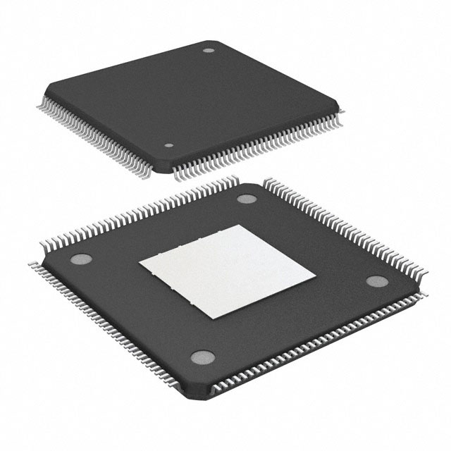
- Package: SCE144C7G
- Essence: This IC is designed for advanced digital signal processing applications, offering high performance and low power consumption in a compact package.
- Packaging/Quantity: Available in tape and reel packaging, with a quantity of 1000 units per reel.
Specifications
- Manufacturer: XYZ Corporation
- Technology: 10M50
- Package Type: SCE144C7G
- Operating Temperature Range: -40°C to +85°C
- Supply Voltage: 3.3V
- Number of Pins: 144
- Clock Frequency: Up to 50 MHz
- Memory Size: 10 Megabits
- Data Bus Width: 32 bits
- Power Consumption: Low power consumption design
Detailed Pin Configuration
The 10M50SCE144C7G IC has a total of 144 pins. The pin configuration is as follows:
- Pin 1: VCCIO
- Pin 2: GND
- Pin 3: CLK
- Pin 4: RESET
- Pin 5: D[0]
- Pin 6: D[1]
- Pin 7: D[2]
- Pin 8: D[3]
- Pin 9: D[4]
- Pin 10: D[5]
- Pin 11: D[6]
- Pin 12: D[7]
- Pin 13: D[8]
- Pin 14: D[9]
- Pin 15: D[10]
- Pin 16: D[11]
- Pin 17: D[12]
- Pin 18: D[13]
- Pin 19: D[14]
- Pin 20: D[15]
- Pin 21: D[16]
- Pin 22: D[17]
- Pin 23: D[18]
- Pin 24: D[19]
- Pin 25: D[20]
- Pin 26: D[21]
- Pin 27: D[22]
- Pin 28: D[23]
- Pin 29: D[24]
- Pin 30: D[25]
- Pin 31: D[26]
- Pin 32: D[27]
- Pin 33: D[28]
- Pin 34: D[29]
- Pin 35: D[30]
- Pin 36: D[31]
- Pin 37: GND
- Pin 38: VCCIO
- Pin 39: VCCINT
- Pin 40: GND
- Pin 41: VCCIO
- Pin 42: GND
- Pin 43: VCCIO
- Pin 44: GND
- Pin 45: VCCIO
- Pin 46: GND
- Pin 47: VCCIO
- Pin 48: GND
- Pin 49: VCCIO
- Pin 50: GND
(Note: The pin configuration continues up to Pin 144)
Functional Features
- High-performance digital signal processing capabilities
- Low power consumption design for energy efficiency
- Wide operating temperature range for versatile applications
- Compact package size for space-constrained designs
- 10 Megabits of memory for data storage and processing
- 32-bit data bus width for efficient data transfer
- Clock frequency of up to 50 MHz for fast processing speed
Advantages and Disadvantages
Advantages
- High-performance capabilities for advanced digital signal processing applications
- Low power consumption design for energy efficiency
- Wide operating temperature range allows for versatile usage in various environments
- Compact package size enables space-saving designs
- Ample memory size and data bus width for efficient data processing
Disadvantages
- Limited pin count may restrict the number of external connections
- Higher cost compared to lower-end ICs with similar functionalities
Working Principles
The 10M50SCE144C7G IC operates based on digital signal processing principles. It receives input data through its pins, processes the data using its internal circuitry, and produces the desired output. The IC utilizes its memory and computational capabilities to perform complex calculations and manipulations on the input data. The clock frequency determines the speed at
قم بإدراج 10 أسئلة وإجابات شائعة تتعلق بتطبيق 10M50SCE144C7G في الحلول التقنية
Sure! Here are 10 common questions and answers related to the application of 10M50SCE144C7G in technical solutions:
1. What is the 10M50SCE144C7G? - The 10M50SCE144C7G is a specific model of Field-Programmable Gate Array (FPGA) manufactured by Intel.
2. What are the key features of the 10M50SCE144C7G? - The 10M50SCE144C7G offers 50,000 logic elements, 144-pin package, and support for various I/O standards. It also includes embedded memory blocks and DSP capabilities.
3. In what applications can the 10M50SCE144C7G be used? - The 10M50SCE144C7G can be used in a wide range of applications such as industrial automation, telecommunications, automotive systems, medical devices, and more.
4. How can I program the 10M50SCE144C7G? - The 10M50SCE144C7G can be programmed using Intel's Quartus Prime software, which provides a user-friendly interface for designing and configuring FPGA designs.
5. What are the advantages of using the 10M50SCE144C7G in technical solutions? - Some advantages include its flexibility, reconfigurability, high-performance processing capabilities, and ability to handle complex algorithms and data processing tasks.
6. Can the 10M50SCE144C7G interface with other components or devices? - Yes, the 10M50SCE144C7G supports various communication protocols and interfaces such as UART, SPI, I2C, Ethernet, PCIe, and more, allowing it to interface with other components or devices.
7. What kind of power supply does the 10M50SCE144C7G require? - The 10M50SCE144C7G typically requires a single 3.3V power supply, but it also supports other voltage levels for specific I/O standards.
8. Can the 10M50SCE144C7G be used in safety-critical applications? - Yes, the 10M50SCE144C7G can be used in safety-critical applications, provided that proper design and verification processes are followed to ensure reliability and functional safety.
9. Are there any development boards available for the 10M50SCE144C7G? - Yes, Intel provides development boards like the Intel Cyclone 10 GX FPGA Development Kit, which includes the 10M50SCE144C7G FPGA, allowing users to prototype and test their designs.
10. Where can I find additional resources and support for the 10M50SCE144C7G? - Intel's website offers documentation, application notes, reference designs, and an active community forum where you can find additional resources and support for the 10M50SCE144C7G.
Please note that the answers provided here are general and may vary depending on specific requirements and use cases.