

5AGXFB1H6F35C6N
Product Overview
Category
The 5AGXFB1H6F35C6N belongs to the category of Field Programmable Gate Arrays (FPGAs).
Use
This FPGA is commonly used in various electronic devices and systems for digital logic implementation, such as communication equipment, industrial control systems, and high-performance computing.
Characteristics
- High-density integration: The 5AGXFB1H6F35C6N offers a large number of programmable logic elements, allowing for complex digital circuit designs.
- Flexible configuration: It can be reprogrammed multiple times to adapt to different application requirements.
- Low power consumption: This FPGA is designed to operate efficiently while minimizing power consumption.
- High-speed performance: It supports high-speed data processing and can handle complex algorithms effectively.
Package
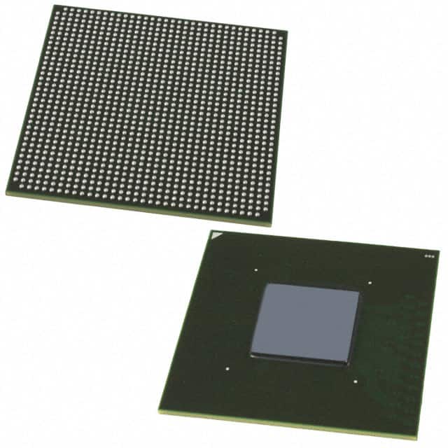
The 5AGXFB1H6F35C6N comes in a compact package that ensures easy integration into electronic systems. The package includes the FPGA chip, which is mounted on a small circuit board.
Essence
The essence of the 5AGXFB1H6F35C6N lies in its ability to provide a highly configurable and flexible digital logic implementation solution. It allows designers to create custom digital circuits without the need for dedicated hardware components.
Packaging/Quantity
The 5AGXFB1H6F35C6N is typically sold individually or in small quantities, depending on the manufacturer's packaging options.
Specifications
- FPGA Family: 5AGXFB1H6
- Logic Elements: 35,000
- Maximum User I/Os: 600
- Embedded Memory: 2,073,600 bits
- Clock Management: PLLs and DLLs
- Operating Voltage: 1.2V
- Package Type: FBGA
- Package Pins: 484
Detailed Pin Configuration
The 5AGXFB1H6F35C6N has a total of 484 pins, each serving a specific purpose in the FPGA's operation. The pin configuration includes input/output pins, power supply pins, clock pins, and configuration pins. A detailed pinout diagram can be found in the product datasheet.
Functional Features
High-Level Integration
The 5AGXFB1H6F35C6N offers a high level of integration, allowing designers to implement complex digital systems on a single chip. It supports various digital logic functions, including arithmetic operations, memory storage, and communication protocols.
Reconfigurability
One of the key features of this FPGA is its reconfigurability. Designers can modify the functionality of the FPGA by reprogramming it, enabling rapid prototyping and design iterations without the need for hardware modifications.
High-Speed Performance
The 5AGXFB1H6F35C6N is designed to operate at high clock frequencies, enabling fast data processing and real-time system response. This feature makes it suitable for applications that require high-performance computing and signal processing.
Low Power Consumption
Despite its high-speed performance, the 5AGXFB1H6F35C6N is optimized for low power consumption. It incorporates power-saving techniques such as dynamic power management and clock gating, ensuring efficient operation while minimizing energy usage.
Advantages and Disadvantages
Advantages
- High-density integration allows for complex digital circuit designs.
- Flexible reconfigurability enables rapid prototyping and design iterations.
- High-speed performance facilitates real-time data processing.
- Low power consumption ensures energy-efficient operation.
Disadvantages
- Steep learning curve for beginners due to the complexity of FPGA programming.
- Limited availability of comprehensive development tools and resources.
- Higher cost compared to traditional fixed-function integrated circuits.
Working Principles
The 5AGXFB1H6F35C6N operates based on the principles of digital logic implementation using programmable logic elements. It consists of configurable logic blocks (CLBs), interconnect resources, embedded memory, and I/O interfaces. The CLBs can be programmed to perform various logic functions, while the interconnect resources enable communication between different components within the FPGA.
During operation, the FPGA is configured by loading a bitstream that defines the desired functionality into its internal memory. This configuration data determines how the logic elements are interconnected and what operations they perform. Once configured, the FPGA executes the specified digital logic operations in real-time.
Detailed Application Field Plans
The 5AGXFB1H6F35C6N finds applications in various fields, including:
- Communication Equipment: Used in network routers, switches, and wireless base stations for high-speed data processing and protocol handling.
- Industrial Control Systems: Employed in automation systems, robotics, and process control applications for real-time control and monitoring.
- High-Performance Computing: Utilized in super
قم بإدراج 10 أسئلة وإجابات شائعة تتعلق بتطبيق 5AGXFB1H6F35C6N في الحلول التقنية
Sure! Here are 10 common questions and answers related to the application of 5AGXFB1H6F35C6N in technical solutions:
1. What is the 5AGXFB1H6F35C6N? - The 5AGXFB1H6F35C6N is a specific model of field-programmable gate array (FPGA) manufactured by Intel.
2. What are the key features of the 5AGXFB1H6F35C6N? - The 5AGXFB1H6F35C6N offers high-performance processing capabilities, low power consumption, and a large number of programmable logic elements.
3. In what applications can the 5AGXFB1H6F35C6N be used? - The 5AGXFB1H6F35C6N can be used in various applications such as telecommunications, industrial automation, automotive systems, and high-performance computing.
4. How does the 5AGXFB1H6F35C6N contribute to system performance? - The 5AGXFB1H6F35C6N provides hardware acceleration, parallel processing capabilities, and real-time data processing, which can significantly enhance system performance.
5. Can the 5AGXFB1H6F35C6N be reprogrammed? - Yes, the 5AGXFB1H6F35C6N is a field-programmable device, meaning it can be reprogrammed multiple times to adapt to different requirements or updates.
6. What development tools are available for programming the 5AGXFB1H6F35C6N? - Intel Quartus Prime is the primary development tool used for programming and configuring the 5AGXFB1H6F35C6N FPGA.
7. What are the power requirements for the 5AGXFB1H6F35C6N? - The power requirements for the 5AGXFB1H6F35C6N vary depending on the specific application and configuration, but it generally operates at low power levels.
8. Can the 5AGXFB1H6F35C6N interface with other components or devices? - Yes, the 5AGXFB1H6F35C6N supports various communication interfaces such as PCIe, Ethernet, USB, and I2C, allowing it to interface with other components or devices.
9. Are there any limitations or considerations when using the 5AGXFB1H6F35C6N? - Some considerations include the need for expertise in FPGA programming, potential design constraints, and the availability of appropriate support resources.
10. Where can I find more information about the 5AGXFB1H6F35C6N? - You can find more detailed information about the 5AGXFB1H6F35C6N on Intel's official website, including datasheets, user guides, and application notes.
Please note that the answers provided here are general and may vary based on specific use cases or requirements.