

5SGSMD4H1F35I2N
Product Overview
Category
The 5SGSMD4H1F35I2N belongs to the category of Field Programmable Gate Arrays (FPGAs).
Use
This FPGA is designed for high-performance applications that require complex digital logic circuits. It provides a flexible and reconfigurable platform for implementing custom digital designs.
Characteristics
- High-performance FPGA with advanced features
- Reconfigurable architecture allows for flexibility in design implementation
- Supports complex digital logic circuits
- Offers high-speed data processing capabilities
- Provides extensive I/O options for interfacing with external devices
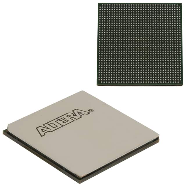
Package
The 5SGSMD4H1F35I2N comes in a compact package that ensures easy integration into electronic systems. The package is designed to provide protection against environmental factors such as moisture, dust, and electrostatic discharge.
Essence
The essence of this FPGA lies in its ability to provide a customizable and versatile solution for implementing digital logic circuits. It enables designers to create complex systems with high performance and flexibility.
Packaging/Quantity
The 5SGSMD4H1F35I2N is typically packaged individually and is available in various quantities depending on the requirements of the user or project.
Specifications
- FPGA Family: Stratix V
- Logic Elements: 115,200
- Embedded Memory: 4,824 Kbits
- Maximum User I/Os: 622
- Operating Voltage: 1.2V
- Maximum Operating Frequency: 500 MHz
- Package Type: F35
- Temperature Range: -40°C to +100°C
Detailed Pin Configuration
The detailed pin configuration of the 5SGSMD4H1F35I2N can be found in the product datasheet provided by the manufacturer. It includes information on the pin names, functions, and electrical characteristics.
Functional Features
- High-speed data processing capabilities
- Configurable logic elements for implementing custom digital designs
- Embedded memory blocks for efficient data storage
- Flexible I/O options for interfacing with external devices
- Support for various communication protocols
- On-chip debugging and testing features
Advantages and Disadvantages
Advantages
- High-performance FPGA suitable for complex applications
- Reconfigurable architecture allows for flexibility in design implementation
- Extensive I/O options enable easy integration with external devices
- Advanced features provide high-speed data processing capabilities
Disadvantages
- Relatively higher cost compared to other programmable logic devices
- Steeper learning curve for beginners due to the complexity of FPGA programming
- Requires specialized tools and software for development and debugging
Working Principles
The 5SGSMD4H1F35I2N operates based on the principles of field-programmable gate arrays. It consists of configurable logic elements, embedded memory blocks, and I/O interfaces. The FPGA can be programmed using hardware description languages (HDLs) such as VHDL or Verilog. Once programmed, the FPGA executes the desired digital logic circuits by routing signals through its configurable elements.
Detailed Application Field Plans
The 5SGSMD4H1F35I2N finds applications in various fields, including:
- Telecommunications: Used in high-speed data transmission systems, network routers, and switches.
- Aerospace and Defense: Employed in radar systems, avionics, and military communication equipment.
- Industrial Automation: Utilized in control systems, robotics, and machine vision applications.
- Medical Devices: Integrated into medical imaging systems, patient monitoring devices, and diagnostic equipment.
- Automotive: Applied in advanced driver-assistance systems (ADAS), infotainment systems, and engine control units.
Detailed and Complete Alternative Models
- 5SGSMD4H2F35I2N
- 5SGSMD4H3F35I2N
- 5SGSMD4H4F35I2N
- 5SGSMD4H5F35I2N
- 5SGSMD4H6F35I2N
These alternative models offer similar features and capabilities to the 5SGSMD4H1F35I2N, but may have variations in terms of logic elements, embedded memory, or I/O options.
In conclusion, the 5SGSMD4H1F35I2N is a high-performance FPGA that provides a flexible and reconfigurable platform for implementing complex digital logic circuits. Its advanced features, extensive I/O options, and customizable nature make it suitable for a wide range of applications across various industries.
قم بإدراج 10 أسئلة وإجابات شائعة تتعلق بتطبيق 5SGSMD4H1F35I2N في الحلول التقنية
Sure! Here are 10 common questions and answers related to the application of 5SGSMD4H1F35I2N in technical solutions:
Q1: What is the 5SGSMD4H1F35I2N? A1: The 5SGSMD4H1F35I2N is a specific model of Field-Programmable Gate Array (FPGA) manufactured by Intel. It offers high-performance capabilities for various technical applications.
Q2: What are the key features of the 5SGSMD4H1F35I2N? A2: The 5SGSMD4H1F35I2N FPGA features a high logic density, advanced DSP capabilities, embedded transceivers, and support for various communication protocols. It also has a large amount of on-chip memory and supports high-speed interfaces.
Q3: In what technical solutions can the 5SGSMD4H1F35I2N be used? A3: The 5SGSMD4H1F35I2N can be used in a wide range of technical solutions, including but not limited to telecommunications, networking, data centers, industrial automation, image processing, and high-performance computing.
Q4: How does the 5SGSMD4H1F35I2N enhance performance in technical solutions? A4: The 5SGSMD4H1F35I2N FPGA provides hardware acceleration, parallel processing, and customizable logic, allowing for optimized performance in various applications. It enables developers to implement complex algorithms and achieve high throughput.
Q5: Can the 5SGSMD4H1F35I2N be programmed using industry-standard tools? A5: Yes, the 5SGSMD4H1F35I2N can be programmed using popular industry-standard tools such as Intel Quartus Prime. These tools provide a user-friendly environment for designing, simulating, and programming the FPGA.
Q6: What are the power requirements for the 5SGSMD4H1F35I2N? A6: The power requirements for the 5SGSMD4H1F35I2N vary depending on the specific implementation and usage scenario. It is recommended to refer to the datasheet and design guidelines provided by Intel for accurate power estimation.
Q7: Can the 5SGSMD4H1F35I2N interface with other components or devices? A7: Yes, the 5SGSMD4H1F35I2N supports various interfaces such as PCIe, Ethernet, USB, DDR memory, and more. It can easily interface with other components or devices in a system, enabling seamless integration into existing solutions.
Q8: Is the 5SGSMD4H1F35I2N suitable for real-time applications? A8: Yes, the 5SGSMD4H1F35I2N is well-suited for real-time applications due to its high-speed processing capabilities, low-latency communication interfaces, and support for parallel processing. It can handle time-critical tasks efficiently.
Q9: Are there any limitations or considerations when using the 5SGSMD4H1F35I2N? A9: While the 5SGSMD4H1F35I2N offers powerful features, it is important to consider factors such as power consumption, thermal management, and board-level design constraints. Proper design practices and guidelines should be followed for optimal performance.
Q10: Where can I find additional resources and support for the 5SGSMD4H1F35I2N? A10: Intel provides comprehensive documentation, datasheets, reference designs, and application notes for the 5SGSMD4H1F35I2N on their official website. Additionally, online forums and communities dedicated to FPGA development can be valuable sources of information and support.