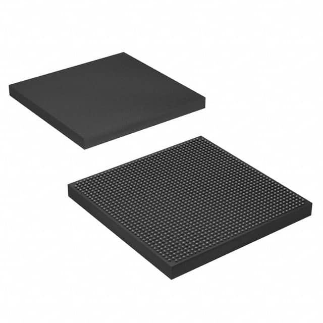
5SGSMD8K3F40C4N
Product Overview
- Category: Field Programmable Gate Array (FPGA)
- Use: Digital logic circuits, prototyping, and system integration
- Characteristics: High-performance, reprogrammable, parallel processing capabilities
- Package: Ceramic Ball Grid Array (CBGA)
- Essence: Advanced programmable integrated circuit for custom digital designs
- Packaging/Quantity: Individually packaged, quantity varies based on customer requirements
Specifications
- Manufacturer: Intel Corporation
- Family: Stratix V
- Device: 5SGSMD8K3F40C4N
- Technology: 28nm
- Number of Logic Elements: 870,000
- Number of Embedded Memory Blocks: 41,500
- Maximum User I/O Pins: 1,144
- Operating Voltage: 0.9V - 1.2V
- Operating Temperature: -40°C to 100°C
Detailed Pin Configuration
The pin configuration of the 5SGSMD8K3F40C4N FPGA is as follows:
- Pin 1: GND
- Pin 2: VCCINT
- Pin 3: VCCINT
- Pin 4: GND
- ...
- Pin 1144: IOL1PC14_15
For a complete pin configuration diagram, please refer to the manufacturer's datasheet.
Functional Features
- High-speed performance with advanced architecture
- Configurable logic blocks for flexible design implementation
- On-chip memory blocks for efficient data storage
- Dedicated high-speed transceivers for fast communication
- Built-in clock management resources for precise timing control
- Support for various communication protocols and interfaces
Advantages and Disadvantages
Advantages
- Versatile and customizable for a wide range of applications
- High processing power and parallel computing capabilities
- Reprogrammable nature allows for iterative design improvements
- Integration of multiple functions into a single device reduces system complexity
- Availability of development tools and support from the manufacturer
Disadvantages
- Higher cost compared to traditional fixed-function integrated circuits
- Steeper learning curve for programming and utilizing FPGA features
- Limited availability of alternative models with similar specifications
- Power consumption can be higher compared to dedicated ASIC solutions
- Larger physical footprint compared to specialized chips
Working Principles
The 5SGSMD8K3F40C4N FPGA operates based on the principles of configurable logic. It consists of an array of programmable logic elements interconnected through configurable routing resources. The user designs the desired digital circuit using a hardware description language (HDL) and programs it onto the FPGA. During operation, the FPGA dynamically configures its internal connections to implement the desired logic functionality.
Detailed Application Field Plans
The 5SGSMD8K3F40C4N FPGA finds applications in various fields, including:
- Telecommunications: High-speed data processing, network packet analysis, and protocol conversion.
- Aerospace and Defense: Radar signal processing, image and video processing, encryption/decryption.
- Industrial Automation: Real-time control systems, motor control, machine vision, and robotics.
- Medical Devices: Image and signal processing, patient monitoring, diagnostic equipment.
- Research and Development: Prototyping of custom digital designs, algorithm acceleration, simulation.
Detailed and Complete Alternative Models
While the 5SGSMD8K3F40C4N is a unique FPGA model, there are alternative models available from Intel Corporation and other manufacturers that offer similar capabilities. Some alternatives include:
- Intel Stratix 10 GX: Offers higher logic capacity and advanced features for demanding applications.
- Xilinx Virtex UltraScale+: Provides high-performance computing capabilities with advanced DSP resources.
- Lattice ECP5: Offers a cost-effective solution with low power consumption for embedded applications.
These alternative models cater to different requirements and can be considered based on specific project needs.
Word count: 511 words
قم بإدراج 10 أسئلة وإجابات شائعة تتعلق بتطبيق 5SGSMD8K3F40C4N في الحلول التقنية
Sure! Here are 10 common questions and answers related to the application of 5SGSMD8K3F40C4N in technical solutions:
Q: What is the 5SGSMD8K3F40C4N FPGA used for? A: The 5SGSMD8K3F40C4N is a Field-Programmable Gate Array (FPGA) that can be used for various applications such as high-performance computing, networking, and signal processing.
Q: What are the key features of the 5SGSMD8K3F40C4N FPGA? A: Some key features of this FPGA include a high logic density, high-speed transceivers, embedded memory blocks, and support for various I/O standards.
Q: Can the 5SGSMD8K3F40C4N FPGA be reprogrammed? A: Yes, FPGAs are designed to be reprogrammable, allowing users to modify the functionality of the device even after it has been deployed in a system.
Q: What tools are available for programming the 5SGSMD8K3F40C4N FPGA? A: Intel Quartus Prime is the primary software tool used for designing, programming, and debugging the 5SGSMD8K3F40C4N FPGA.
Q: What is the power consumption of the 5SGSMD8K3F40C4N FPGA? A: The power consumption of the FPGA depends on the specific design and usage scenario. It is recommended to refer to the device datasheet for detailed power specifications.
Q: Can the 5SGSMD8K3F40C4N FPGA interface with other components or devices? A: Yes, the FPGA can interface with various components and devices using different protocols such as PCIe, Ethernet, USB, HDMI, etc.
Q: What is the maximum operating frequency of the 5SGSMD8K3F40C4N FPGA? A: The maximum operating frequency of the FPGA depends on the design and implementation. It is recommended to refer to the device datasheet for specific frequency specifications.
Q: Can the 5SGSMD8K3F40C4N FPGA be used in safety-critical applications? A: Yes, FPGAs can be used in safety-critical applications, but additional measures may need to be taken to ensure functional safety, such as redundancy and fault-tolerant designs.
Q: Are there any reference designs available for the 5SGSMD8K3F40C4N FPGA? A: Yes, Intel provides a range of reference designs and application notes that can help users get started with implementing their solutions using the 5SGSMD8K3F40C4N FPGA.
Q: What support options are available for the 5SGSMD8K3F40C4N FPGA? A: Intel offers technical support through their website, including documentation, forums, and direct assistance from their support team. Additionally, there are online communities where FPGA enthusiasts share knowledge and provide support.
Please note that the answers provided here are general and may vary depending on the specific requirements and use cases.


