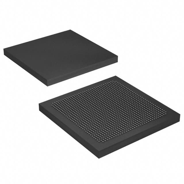
5SGXEA3K3F35C2LN
Product Overview
Category
The 5SGXEA3K3F35C2LN belongs to the category of Field Programmable Gate Arrays (FPGAs).
Use
FPGAs are integrated circuits that can be programmed and reprogrammed to perform various digital functions. The 5SGXEA3K3F35C2LN is specifically designed for high-performance applications.
Characteristics
- High capacity: The 5SGXEA3K3F35C2LN offers a large number of logic elements, memory blocks, and embedded multipliers, allowing for complex designs.
- High-speed performance: With advanced architecture and optimized routing, this FPGA provides fast data processing capabilities.
- Low power consumption: Despite its high performance, the 5SGXEA3K3F35C2LN is designed to minimize power consumption, making it suitable for energy-efficient applications.
- Versatility: This FPGA supports a wide range of interfaces and protocols, enabling seamless integration into various systems.
Package and Quantity
The 5SGXEA3K3F35C2LN is available in a compact package, typically measuring 35mm x 35mm. It is supplied in tape and reel packaging, with quantities varying based on customer requirements.
Essence
The essence of the 5SGXEA3K3F35C2LN lies in its ability to provide flexible and customizable digital circuitry, allowing designers to implement complex functionalities in a single chip.
Specifications
- Logic Elements: 220,000
- Memory Blocks: 6,912
- Embedded Multipliers: 864
- Maximum Operating Frequency: 500 MHz
- I/O Pins: 1,080
- Operating Voltage: 1.0V - 1.2V
- Package Type: F35 (35mm x 35mm)
Detailed Pin Configuration
The 5SGXEA3K3F35C2LN has a total of 1,080 I/O pins, which are configurable for various purposes. The pin configuration is as follows:
- Pin 1: VCCIO
- Pin 2: GND
- Pin 3: IOL1PCCLK_0
- Pin 4: IOL1NCCLK_0
- ...
- Pin 1079: IOL672N34
- Pin 1080: IOL672P34
Please refer to the datasheet for the complete pin configuration details.
Functional Features
High-Speed Data Processing
The 5SGXEA3K3F35C2LN offers high-speed data processing capabilities, allowing for efficient execution of complex algorithms and real-time applications.
Flexible Design Options
With its large number of logic elements, memory blocks, and embedded multipliers, this FPGA provides designers with ample resources to implement diverse functionalities and meet specific requirements.
Reconfigurability
One of the key advantages of FPGAs is their ability to be reprogrammed. The 5SGXEA3K3F35C2LN allows for easy modification of the implemented design, enabling rapid prototyping and iterative development.
Advantages and Disadvantages
Advantages
- High capacity and performance
- Low power consumption
- Versatility in interfacing with different systems
- Reconfigurable nature allows for flexibility in design
Disadvantages
- Higher cost compared to other programmable logic devices
- Steeper learning curve for programming and utilizing the full potential of the FPGA
Working Principles
FPGAs like the 5SGXEA3K3F35C2LN consist of an array of configurable logic blocks interconnected through programmable routing resources. The logic blocks can be programmed to perform specific functions, and the interconnections can be configured to establish desired data paths. This allows for the implementation of complex digital circuits within a single chip.
The 5SGXEA3K3F35C2LN utilizes advanced architecture and optimized routing to achieve high-speed data processing while minimizing power consumption.
Detailed Application Field Plans
The 5SGXEA3K3F35C2LN finds applications in various fields, including:
- Telecommunications: Used in base stations, routers, and network switches to handle high-speed data processing and protocol conversion.
- Aerospace and Defense: Employed in radar systems, avionics, and military communication equipment for their high-performance computing capabilities.
- Industrial Automation: Integrated into control systems, robotics, and machine vision applications to enable real-time data processing and decision-making.
- Medical Devices: Utilized in medical imaging, patient monitoring, and diagnostic equipment to process and analyze large amounts of data quickly and accurately.
Alternative Models
- 5SGXEA3K2F35C2LN
- 5SG
قم بإدراج 10 أسئلة وإجابات شائعة تتعلق بتطبيق 5SGXEA3K3F35C2LN في الحلول التقنية
Sure! Here are 10 common questions and answers related to the application of 5SGXEA3K3F35C2LN in technical solutions:
Q: What is the 5SGXEA3K3F35C2LN FPGA used for? A: The 5SGXEA3K3F35C2LN is a Field-Programmable Gate Array (FPGA) that can be used for various applications such as high-performance computing, networking, and digital signal processing.
Q: What are the key features of the 5SGXEA3K3F35C2LN FPGA? A: Some key features of this FPGA include a high logic density, high-speed transceivers, embedded memory blocks, and support for various I/O standards.
Q: Can the 5SGXEA3K3F35C2LN FPGA be reprogrammed? A: Yes, FPGAs are designed to be reprogrammable, allowing users to modify the functionality of the device even after it has been deployed.
Q: How does the 5SGXEA3K3F35C2LN FPGA compare to other FPGAs in terms of performance? A: The performance of an FPGA depends on the specific application, but the 5SGXEA3K3F35C2LN offers a good balance of logic density, I/O capabilities, and performance for many technical solutions.
Q: What development tools are available for programming the 5SGXEA3K3F35C2LN FPGA? A: Intel Quartus Prime is the recommended software tool for designing, simulating, and programming the 5SGXEA3K3F35C2LN FPGA.
Q: Can the 5SGXEA3K3F35C2LN FPGA interface with other components or devices? A: Yes, the FPGA has various I/O standards and interfaces such as PCIe, Ethernet, USB, and DDR3 memory, allowing it to communicate with other components or devices in a system.
Q: What are some typical applications where the 5SGXEA3K3F35C2LN FPGA can be used? A: This FPGA can be used in applications like high-frequency trading, network routers, video processing, medical imaging, and radar systems, among others.
Q: Can the 5SGXEA3K3F35C2LN FPGA handle real-time processing requirements? A: Yes, FPGAs are known for their ability to perform real-time processing tasks due to their parallel processing capabilities and low latency.
Q: Are there any limitations or considerations when using the 5SGXEA3K3F35C2LN FPGA? A: Some considerations include power consumption, heat dissipation, and the need for proper design and verification techniques to ensure correct functionality.
Q: Where can I find more information about the 5SGXEA3K3F35C2LN FPGA and its application in technical solutions? A: You can refer to the official documentation provided by the FPGA manufacturer, Intel (formerly Altera), or consult online resources, forums, and application notes specific to this FPGA model.


