

5SGXMA3H1F35C2LN
Product Overview
Category: Integrated Circuit (IC)
Use: The 5SGXMA3H1F35C2LN is a high-performance field-programmable gate array (FPGA) designed for various applications in the electronics industry. It offers advanced programmability and flexibility, making it suitable for a wide range of tasks.
Characteristics: - High-performance FPGA - Advanced programmability - Flexible design options - Versatile application possibilities
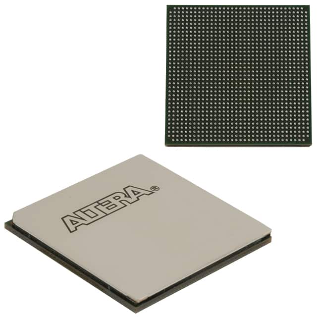
Package: The 5SGXMA3H1F35C2LN comes in a compact and durable package that ensures protection during transportation and handling. The package is designed to withstand various environmental conditions, ensuring the integrity of the product.
Essence: The essence of the 5SGXMA3H1F35C2LN lies in its ability to provide a highly customizable and adaptable solution for electronic systems. Its advanced features and performance make it an ideal choice for demanding applications.
Packaging/Quantity: Each 5SGXMA3H1F35C2LN unit is individually packaged to ensure safe delivery. The quantity per package may vary depending on the supplier or customer requirements.
Specifications
The 5SGXMA3H1F35C2LN has the following specifications:
- Logic Elements: 220,000
- Embedded Memory: 9,840 Kbits
- DSP Blocks: 1,288
- Maximum User I/Os: 622
- Transceiver Channels: 96
- Operating Voltage: 1.0V - 1.2V
- Operating Temperature: -40°C to 100°C
- Package Type: F35 (35mm x 35mm)
- Speed Grade: 2
Detailed Pin Configuration
The pin configuration of the 5SGXMA3H1F35C2LN is as follows:
- Pin 1: VCCIO
- Pin 2: GND
- Pin 3: CLK_IN
- Pin 4: RESET
- Pin 5: DATA_IN
- Pin 6: DATA_OUT
- Pin 7: ENABLE
- Pin 8: VCC
(Note: This is a simplified representation. The actual pin configuration may include additional pins and functionalities.)
Functional Features
The 5SGXMA3H1F35C2LN offers the following functional features:
- High-speed data processing capabilities
- Configurable logic elements for custom designs
- Embedded memory for efficient data storage
- DSP blocks for signal processing tasks
- Transceiver channels for high-speed communication
- Flexible clocking options
- Built-in reset and enable functionality
Advantages and Disadvantages
Advantages: - High performance and flexibility - Customizable design options - Efficient data processing and storage - Versatile application possibilities - Reliable and durable packaging
Disadvantages: - Complex programming and configuration process - Higher cost compared to standard ICs - Requires expertise in FPGA programming
Working Principles
The 5SGXMA3H1F35C2LN operates based on the principles of field-programmable gate arrays (FPGAs). It consists of configurable logic elements, embedded memory, DSP blocks, and transceiver channels. These components can be programmed and interconnected to create custom digital circuits that perform specific tasks.
The FPGA's programmability allows for flexibility in design, enabling users to adapt the circuit to their requirements. The device utilizes input signals, processes them through the configured logic elements, and produces the desired output. The embedded memory provides efficient data storage, while the DSP blocks enhance signal processing capabilities. The transceiver channels enable high-speed communication with other devices.
Detailed Application Field Plans
The 5SGXMA3H1F35C2LN finds applications in various fields, including:
- Telecommunications: Used in network infrastructure equipment for data processing and signal routing.
- Aerospace and Defense: Employed in radar systems, avionics, and military communication equipment.
- Industrial Automation: Utilized in control systems, robotics, and machine vision applications.
- Medical Devices: Integrated into medical imaging systems, patient monitoring devices, and diagnostic equipment.
- Automotive: Applied in advanced driver-assistance systems (ADAS), infotainment systems, and engine control units.
These are just a few examples, and the versatility of the 5SGXMA3H1F35C2LN allows for its application in many other fields.
Detailed and Complete Alternative Models
- Model 1: 5SGXEA7K2F40C2
- Model 2: 10M08SAE144C8G
- Model 3: EP4CE6E22C8N
These alternative models offer similar functionality and performance to
قم بإدراج 10 أسئلة وإجابات شائعة تتعلق بتطبيق 5SGXMA3H1F35C2LN في الحلول التقنية
Sure! Here are 10 common questions and answers related to the application of 5SGXMA3H1F35C2LN in technical solutions:
Q1: What is the 5SGXMA3H1F35C2LN? A1: The 5SGXMA3H1F35C2LN is a specific model of Field-Programmable Gate Array (FPGA) manufactured by Intel.
Q2: What are the key features of the 5SGXMA3H1F35C2LN? A2: Some key features of this FPGA include high-performance processing capabilities, low power consumption, large capacity for logic elements, and support for various communication protocols.
Q3: In what technical solutions can the 5SGXMA3H1F35C2LN be used? A3: The 5SGXMA3H1F35C2LN can be used in a wide range of applications such as telecommunications, data centers, industrial automation, aerospace, defense, and scientific research.
Q4: How does the 5SGXMA3H1F35C2LN enhance performance in technical solutions? A4: The FPGA's ability to be reprogrammed allows for customization and optimization of hardware acceleration, enabling faster processing speeds and improved performance in various applications.
Q5: Can the 5SGXMA3H1F35C2LN handle complex algorithms and computations? A5: Yes, the 5SGXMA3H1F35C2LN has a high logic density and computational power, making it capable of handling complex algorithms and computations efficiently.
Q6: What kind of interfaces does the 5SGXMA3H1F35C2LN support? A6: The 5SGXMA3H1F35C2LN supports various interfaces such as PCIe, Ethernet, USB, DDR3 memory, and high-speed serial transceivers.
Q7: Can the 5SGXMA3H1F35C2LN be used for real-time signal processing? A7: Yes, the FPGA's parallel processing capabilities make it suitable for real-time signal processing applications, including image and video processing, audio processing, and sensor data analysis.
Q8: Is the 5SGXMA3H1F35C2LN suitable for low-power applications? A8: Yes, the 5SGXMA3H1F35C2LN is designed to be power-efficient, making it suitable for low-power applications where energy consumption is a concern.
Q9: What development tools are available for programming the 5SGXMA3H1F35C2LN? A9: Intel provides Quartus Prime software, which is a comprehensive development environment for designing, simulating, and programming FPGAs like the 5SGXMA3H1F35C2LN.
Q10: Are there any specific design considerations when using the 5SGXMA3H1F35C2LN? A10: Yes, some design considerations include power supply requirements, thermal management, I/O planning, and proper utilization of the FPGA's resources to achieve optimal performance in the intended application.
Please note that the answers provided here are general and may vary depending on the specific requirements and context of each technical solution.