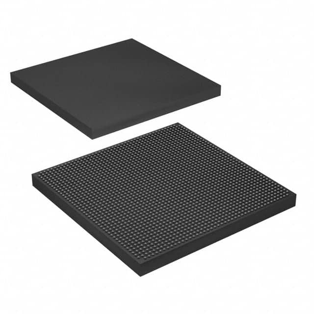
5SGXMA7N3F45C4
Product Overview
Category
The 5SGXMA7N3F45C4 belongs to the category of Field Programmable Gate Arrays (FPGAs).
Use
This FPGA is designed for high-performance applications that require complex digital logic circuits. It provides a flexible and reconfigurable hardware platform for various electronic systems.
Characteristics
- High-speed processing capabilities
- Large number of programmable logic elements
- On-chip memory resources
- Support for various communication protocols
- Low power consumption
- Scalability for future upgrades
Package
The 5SGXMA7N3F45C4 comes in a compact package suitable for integration into electronic devices. The package ensures protection against environmental factors such as temperature, humidity, and electromagnetic interference.
Essence
The essence of the 5SGXMA7N3F45C4 lies in its ability to implement complex digital logic functions through programming. It offers a versatile solution for system designers to create custom hardware designs without the need for dedicated integrated circuits.
Packaging/Quantity
The 5SGXMA7N3F45C4 is typically packaged individually and is available in various quantities depending on the requirements of the customer or project.
Specifications
- Logic Elements: 220,000
- Embedded Memory: 8,400 Kbits
- DSP Blocks: 1,526
- Maximum User I/Os: 622
- Transceivers: 48
- Operating Voltage: 1.2V
- Operating Temperature Range: -40°C to 100°C
- Package Type: FCBGA
- Package Pins: 780
Detailed Pin Configuration
The 5SGXMA7N3F45C4 has a total of 780 pins, each serving a specific purpose within the FPGA. The pin configuration includes input/output pins, power supply pins, clock pins, and configuration pins. A detailed pinout diagram can be found in the product datasheet.
Functional Features
- High-speed data processing capabilities
- Configurable logic elements for custom designs
- On-chip memory resources for data storage
- Support for various communication protocols (e.g., PCIe, Ethernet)
- Built-in digital signal processing blocks for signal manipulation
- Flexible clock management resources for precise timing control
Advantages and Disadvantages
Advantages
- Flexibility to implement custom hardware designs
- Reconfigurability for future upgrades or modifications
- High-performance computing capabilities
- Lower development costs compared to dedicated integrated circuits
- Shorter time-to-market for electronic systems
Disadvantages
- Steeper learning curve for programming and utilizing FPGA features
- Higher power consumption compared to specialized ASICs
- Limited availability of alternative models with similar specifications
Working Principles
The 5SGXMA7N3F45C4 operates based on the principles of reconfigurable computing. It consists of a matrix of programmable logic elements interconnected through configurable routing resources. These logic elements can be programmed to perform specific functions, allowing the FPGA to adapt to different application requirements.
Detailed Application Field Plans
The 5SGXMA7N3F45C4 finds applications in various fields, including:
- Telecommunications: Used in base stations, routers, and network switches for high-speed data processing and protocol handling.
- Aerospace and Defense: Employed in radar systems, avionics, and military communication equipment for their high-performance computing capabilities.
- Industrial Automation: Utilized in control systems, robotics, and machine vision applications for real-time data processing and control.
- Medical Devices: Integrated into medical imaging systems, patient monitoring devices, and diagnostic equipment for advanced signal processing and image analysis.
- Automotive: Used in advanced driver assistance systems (ADAS), infotainment systems, and engine control units for their processing power and flexibility.
Detailed and Complete Alternative Models
While the 5SGXMA7N3F45C4 is a highly capable FPGA, there are alternative models available with similar specifications. Some notable alternatives include:
- Xilinx Virtex UltraScale+ VU9P
- Intel Stratix 10 GX 2800
- Lattice ECP5-85
- Microchip PolarFire MPF300TS
These alternatives offer comparable features and performance, providing designers with options based on their specific project requirements.
In conclusion, the 5SGXMA7N3F45C4 is a powerful FPGA that offers high-performance computing capabilities, flexibility, and reconfigurability. It finds applications in various industries and can be used to implement complex digital logic circuits efficiently.
قم بإدراج 10 أسئلة وإجابات شائعة تتعلق بتطبيق 5SGXMA7N3F45C4 في الحلول التقنية
Sure! Here are 10 common questions and answers related to the application of 5SGXMA7N3F45C4 in technical solutions:
Question: What is the 5SGXMA7N3F45C4 FPGA used for?
Answer: The 5SGXMA7N3F45C4 FPGA is a high-performance field-programmable gate array (FPGA) that can be used in various applications such as telecommunications, industrial automation, and high-performance computing.Question: What are the key features of the 5SGXMA7N3F45C4 FPGA?
Answer: Some key features of this FPGA include a large number of logic elements, high-speed transceivers, embedded memory blocks, and support for various I/O standards.Question: Can the 5SGXMA7N3F45C4 FPGA handle high-speed data transmission?
Answer: Yes, this FPGA is equipped with high-speed transceivers that can support data rates up to 28 Gbps, making it suitable for applications requiring fast data transmission.Question: How much logic capacity does the 5SGXMA7N3F45C4 FPGA offer?
Answer: This FPGA has a logic capacity of approximately 476,000 logic elements, allowing for the implementation of complex digital designs.Question: Can the 5SGXMA7N3F45C4 FPGA be reprogrammed?
Answer: Yes, FPGAs are designed to be reprogrammable, including the 5SGXMA7N3F45C4. This allows for flexibility in design iterations and updates.Question: What kind of memory resources does the 5SGXMA7N3F45C4 FPGA provide?
Answer: This FPGA offers various types of memory resources, including embedded memory blocks (RAM), distributed memory, and external memory interfaces.Question: Is the 5SGXMA7N3F45C4 FPGA suitable for real-time signal processing?
Answer: Yes, this FPGA is capable of handling real-time signal processing tasks due to its high-speed transceivers and parallel processing capabilities.Question: Can the 5SGXMA7N3F45C4 FPGA interface with other devices or systems?
Answer: Absolutely! This FPGA supports various I/O standards, such as LVDS, PCIe, Ethernet, and DDR3/DDR4 memory interfaces, allowing seamless integration with other devices or systems.Question: What development tools are available for programming the 5SGXMA7N3F45C4 FPGA?
Answer: Intel Quartus Prime is the recommended development tool for programming and configuring the 5SGXMA7N3F45C4 FPGA. It provides a comprehensive design environment for FPGA development.Question: Are there any reference designs or application notes available for the 5SGXMA7N3F45C4 FPGA?
Answer: Yes, Intel (formerly Altera) provides a wide range of reference designs, application notes, and documentation to assist users in implementing the 5SGXMA7N3F45C4 FPGA in their technical solutions. These resources can be found on their official website.


