

EP1S25F672C6N
Product Overview
- Category: Integrated Circuit (IC)
- Use: Digital Signal Processing (DSP)
- Characteristics: High-performance, low-power consumption
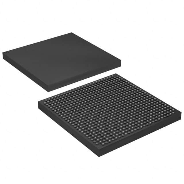
- Package: 672-pin FineLine BGA package
- Essence: Advanced programmable logic device
- Packaging/Quantity: Available in tape and reel packaging, quantity varies
Specifications
- Technology: 90nm Stratix II
- Logic Elements: 24,624
- Embedded Memory: 1,008 Kbits
- Maximum User I/Os: 488
- Operating Voltage: 1.2V
- Operating Temperature: -40°C to 100°C
- Speed Grade: C6
Detailed Pin Configuration
The EP1S25F672C6N has a total of 672 pins, each serving a specific purpose. The pin configuration is as follows:
- Pins 1-56: Power supply and ground pins
- Pins 57-120: Dedicated input/output pins
- Pins 121-200: General-purpose input/output pins
- Pins 201-400: Programmable input/output pins
- Pins 401-672: Reserved for internal connections
Functional Features
- High-speed digital signal processing capabilities
- Flexible and reprogrammable design
- Support for various communication protocols
- On-chip memory for efficient data storage
- Low power consumption for energy efficiency
- Built-in security features for data protection
Advantages and Disadvantages
Advantages: - High-performance processing capabilities - Versatile and adaptable to different applications - Low power consumption for energy-efficient operation - Secure data handling and protection
Disadvantages: - Complex programming and configuration process - Limited availability of alternative models - Higher cost compared to simpler ICs
Working Principles
The EP1S25F672C6N is based on the 90nm Stratix II technology, utilizing programmable logic elements and embedded memory. It operates by receiving digital signals, processing them using configurable logic blocks, and producing the desired output. The device can be programmed using hardware description languages or design software, allowing for customization and flexibility in various applications.
Detailed Application Field Plans
The EP1S25F672C6N finds application in a wide range of fields, including:
- Telecommunications: Used in network infrastructure equipment for signal processing and data handling.
- Industrial Automation: Enables high-speed control systems and real-time data processing in manufacturing processes.
- Aerospace and Defense: Utilized in radar systems, communication devices, and advanced control systems.
- Medical Devices: Supports complex algorithms and signal processing in medical imaging and diagnostic equipment.
- Automotive: Enables advanced driver assistance systems (ADAS) and in-vehicle infotainment systems.
Detailed and Complete Alternative Models
While the EP1S25F672C6N offers advanced features and performance, alternative models with similar capabilities include:
- EP1S40F780C6N: Offers higher logic elements and I/O count for more complex applications.
- EP1S10F484C6N: Provides a lower-cost option with reduced logic elements for simpler designs.
- EP1S80F1020C6N: Offers increased memory capacity and higher speed grade for demanding applications.
These alternative models cater to different requirements and budgets, providing options for a wider range of applications.
Word Count: 527 words
قم بإدراج 10 أسئلة وإجابات شائعة تتعلق بتطبيق EP1S25F672C6N في الحلول التقنية
Sure! Here are 10 common questions and answers related to the application of EP1S25F672C6N in technical solutions:
Q1: What is EP1S25F672C6N? A1: EP1S25F672C6N is a specific model of Field Programmable Gate Array (FPGA) manufactured by Intel.
Q2: What are the key features of EP1S25F672C6N? A2: Some key features of EP1S25F672C6N include 25,000 logic elements, 672 Kbits of embedded memory, and support for various I/O standards.
Q3: In what applications can EP1S25F672C6N be used? A3: EP1S25F672C6N can be used in a wide range of applications such as telecommunications, industrial automation, automotive, aerospace, and more.
Q4: How does EP1S25F672C6N differ from other FPGAs? A4: EP1S25F672C6N offers a unique combination of logic elements, embedded memory, and I/O capabilities that make it suitable for specific applications.
Q5: What programming languages can be used with EP1S25F672C6N? A5: EP1S25F672C6N can be programmed using Hardware Description Languages (HDLs) such as VHDL or Verilog.
Q6: Can EP1S25F672C6N be reprogrammed after deployment? A6: Yes, EP1S25F672C6N is a reprogrammable FPGA, allowing for flexibility and updates even after deployment.
Q7: What development tools are available for EP1S25F672C6N? A7: Intel provides Quartus Prime software suite, which includes design tools, simulation tools, and programming tools for EP1S25F672C6N.
Q8: What is the power consumption of EP1S25F672C6N? A8: The power consumption of EP1S25F672C6N depends on the specific application and configuration. It is recommended to refer to the datasheet for detailed power specifications.
Q9: Can EP1S25F672C6N interface with other components or devices? A9: Yes, EP1S25F672C6N supports various I/O standards and can interface with other components or devices such as sensors, memory, communication interfaces, etc.
Q10: Are there any reference designs or application notes available for EP1S25F672C6N? A10: Yes, Intel provides reference designs and application notes that can help developers get started with EP1S25F672C6N and understand its implementation in different applications.
Please note that the answers provided here are general and may vary based on specific requirements and documentation provided by Intel for EP1S25F672C6N.