

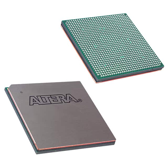
EP1S40F1020C6N
Basic Information Overview
- Category: Programmable Logic Device (PLD)
- Use: EP1S40F1020C6N is a PLD used for digital logic design and implementation.
- Characteristics:
- High-performance device with low power consumption.
- Offers high-speed performance and flexibility in designing complex digital circuits.
- Can be reprogrammed multiple times to accommodate changes in the design.
- Package: The EP1S40F1020C6N comes in a C6N package.
- Essence: EP1S40F1020C6N is an essential component for implementing digital logic designs efficiently.
Specifications
- Number of Logic Elements: 40,000
- Maximum Frequency: 500 MHz
- Number of I/O Pins: 1,020
- Operating Voltage: 3.3V
- Technology: Field-Programmable Gate Array (FPGA)
Detailed Pin Configuration
The EP1S40F1020C6N has a total of 1,020 pins, which are divided into different categories: - Input Pins: These pins receive signals from external devices or other components. - Output Pins: These pins transmit signals to external devices or other components. - Bidirectional Pins: These pins can function as both input and output pins. - Power Pins: These pins provide power supply to the device. - Ground Pins: These pins are connected to the ground for proper functioning.
Functional Features
- High-Speed Performance: EP1S40F1020C6N offers fast operation, making it suitable for applications requiring quick response times.
- Flexibility: The device allows for easy reprogramming, enabling designers to make changes to the logic design without replacing the hardware.
- Low Power Consumption: EP1S40F1020C6N is designed to consume minimal power, making it energy-efficient.
- Large Logic Capacity: With 40,000 logic elements, the device can handle complex digital circuit designs.
Advantages and Disadvantages
Advantages: - High-performance and flexibility in designing digital circuits. - Reprogrammable nature allows for design changes without hardware replacement. - Low power consumption contributes to energy efficiency. - Large logic capacity enables handling of complex designs.
Disadvantages: - Relatively high cost compared to other programmable logic devices. - Requires expertise in digital logic design for optimal utilization. - Limited availability of alternative models may restrict design options.
Working Principles
EP1S40F1020C6N is based on Field-Programmable Gate Array (FPGA) technology. It consists of a matrix of configurable logic blocks interconnected through programmable interconnects. The device can be programmed using Hardware Description Languages (HDLs) like VHDL or Verilog. Once programmed, the EP1S40F1020C6N executes the desired logic functions based on the input signals received.
Detailed Application Field Plans
EP1S40F1020C6N finds applications in various fields, including: - Digital Signal Processing (DSP) - Communication Systems - Industrial Automation - Robotics - Aerospace and Defense - Automotive Electronics
Detailed and Complete Alternative Models
While EP1S40F1020C6N is a popular choice, there are alternative models available from different manufacturers. Some notable alternatives include: - Xilinx Virtex-7 FPGA Series - Altera Cyclone V FPGA Series - Lattice ECP5 FPGA Series - Microsemi SmartFusion2 FPGA Series
These alternative models offer similar functionality and can be considered based on specific project requirements.
Word count: 346 words
قم بإدراج 10 أسئلة وإجابات شائعة تتعلق بتطبيق EP1S40F1020C6N في الحلول التقنية
Sure! Here are 10 common questions and answers related to the application of EP1S40F1020C6N in technical solutions:
Q1: What is EP1S40F1020C6N? A1: EP1S40F1020C6N is a field-programmable gate array (FPGA) manufactured by Intel. It is designed for various applications in digital logic circuits.
Q2: What are the key features of EP1S40F1020C6N? A2: Some key features of EP1S40F1020C6N include 40,000 logic elements, 1,020 Kbits of embedded memory, six high-speed transceivers, and support for various I/O standards.
Q3: What are the typical applications of EP1S40F1020C6N? A3: EP1S40F1020C6N can be used in a wide range of applications such as telecommunications, industrial automation, automotive electronics, medical devices, and aerospace systems.
Q4: How can EP1S40F1020C6N be programmed? A4: EP1S40F1020C6N can be programmed using hardware description languages (HDLs) like VHDL or Verilog. The programming can be done using Intel's Quartus Prime software.
Q5: What is the maximum operating frequency of EP1S40F1020C6N? A5: The maximum operating frequency of EP1S40F1020C6N depends on the design and implementation. However, it can typically operate at frequencies up to several hundred megahertz.
Q6: Can EP1S40F1020C6N interface with other components or devices? A6: Yes, EP1S40F1020C6N supports various I/O standards and can interface with other components or devices such as sensors, memory modules, communication interfaces, and more.
Q7: Does EP1S40F1020C6N have built-in security features? A7: Yes, EP1S40F1020C6N provides built-in security features like bitstream encryption, design separation, and configuration protection to ensure the integrity of the design.
Q8: Can EP1S40F1020C6N be used in safety-critical applications? A8: Yes, EP1S40F1020C6N can be used in safety-critical applications. However, it is important to follow industry-specific safety guidelines and perform thorough testing and verification.
Q9: What are the power requirements for EP1S40F1020C6N? A9: EP1S40F1020C6N requires a supply voltage of 3.3V and has low power consumption. The exact power requirements may vary depending on the design and operating conditions.
Q10: Are there any development boards available for EP1S40F1020C6N? A10: Yes, Intel offers development boards specifically designed for EP1S40F1020C6N, which provide a convenient platform for prototyping and testing FPGA-based solutions.
Please note that these answers are general and may vary based on specific requirements and application scenarios.