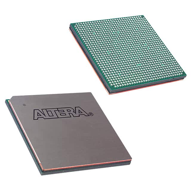
EP1S80F1020C6
Product Overview
- Category: Integrated Circuit (IC)
- Use: Programmable Logic Device (PLD)
- Characteristics: High-performance, low-power consumption
- Package: C6 package
- Essence: Versatile programmable logic solution
- Packaging/Quantity: Single unit packaging
Specifications
- Model: EP1S80F1020C6
- Technology: Field-Programmable Gate Array (FPGA)
- Logic Elements: 80,000
- Speed Grade: 6
- I/O Pins: 1,020
- Operating Voltage: 3.3V
- Package Type: Ceramic Column Grid Array (CCGA)
Detailed Pin Configuration
The EP1S80F1020C6 has a total of 1,020 pins, which are organized into various functional groups. The pin configuration is as follows:
- Power Supply Pins: VCCINT, VCCAUX, VCCO, GND
- Configuration Pins: CONFDONE, CONFSEL, CONFCLK, CONFDATA
- Clock Pins: CLK0, CLK1, CLK2, ...
- Input/Output Pins: IO0, IO1, IO2, ...
- Special Function Pins: JTAGTCK, JTAGTMS, JTAGTDI, JTAGTDO
For a complete pinout diagram and detailed pin descriptions, refer to the product datasheet.
Functional Features
- High-density programmable logic device with a large number of logic elements
- Low power consumption for energy-efficient operation
- Flexible I/O capabilities for versatile connectivity options
- Advanced configuration options for customization
- Support for various communication protocols and interfaces
- Built-in memory blocks for efficient data storage and retrieval
Advantages and Disadvantages
Advantages: - High performance and speed - Versatility in application - Low power consumption - Extensive I/O capabilities
Disadvantages: - Complex programming and configuration process - Higher cost compared to simpler logic devices - Limited availability of alternative models
Working Principles
The EP1S80F1020C6 is based on FPGA technology, which allows for the reconfiguration of its internal logic elements. It consists of a large number of configurable logic blocks interconnected through programmable interconnects. The device can be programmed using hardware description languages (HDL) or design software tools. Once programmed, the EP1S80F1020C6 performs the desired logic functions based on the user's design.
Detailed Application Field Plans
The EP1S80F1020C6 finds applications in various fields, including:
- Telecommunications: Used in network equipment for data processing and routing.
- Industrial Automation: Employed in control systems for factory automation and robotics.
- Aerospace and Defense: Utilized in avionics systems for signal processing and control.
- Medical Devices: Integrated into medical equipment for data acquisition and analysis.
- Automotive Electronics: Incorporated in automotive control units for enhanced functionality.
Detailed and Complete Alternative Models
While the EP1S80F1020C6 is a highly capable PLD, there are alternative models available from other manufacturers that offer similar functionality. Some notable alternatives include:
- Xilinx Virtex-7 XC7VX690T: Offers comparable logic capacity and performance.
- Altera Stratix V 5SGXEA7N2F45C2: Provides similar features and high-speed interfaces.
- Lattice ECP5-85: A lower-cost option with moderate logic capacity.
These alternative models can be considered based on specific project requirements and budget constraints.
Word count: 408 words
قم بإدراج 10 أسئلة وإجابات شائعة تتعلق بتطبيق EP1S80F1020C6 في الحلول التقنية
Sure! Here are 10 common questions and answers related to the application of EP1S80F1020C6 in technical solutions:
Q1: What is EP1S80F1020C6? A1: EP1S80F1020C6 is a field-programmable gate array (FPGA) manufactured by Intel. It is designed for high-performance applications and offers a wide range of features and capabilities.
Q2: What are the key features of EP1S80F1020C6? A2: Some key features of EP1S80F1020C6 include 80,000 logic elements, 1,020 user I/O pins, embedded memory blocks, high-speed transceivers, and support for various communication protocols.
Q3: What are the typical applications of EP1S80F1020C6? A3: EP1S80F1020C6 is commonly used in applications such as telecommunications, networking, industrial automation, video processing, and high-performance computing.
Q4: How can EP1S80F1020C6 be programmed? A4: EP1S80F1020C6 can be programmed using Intel's Quartus Prime software, which provides a graphical interface for designing, simulating, and programming the FPGA.
Q5: Can EP1S80F1020C6 be used in safety-critical applications? A5: Yes, EP1S80F1020C6 can be used in safety-critical applications. However, it is important to follow proper design practices and perform thorough testing and verification to ensure reliability and safety.
Q6: Does EP1S80F1020C6 support high-speed serial communication? A6: Yes, EP1S80F1020C6 has built-in high-speed transceivers that support various serial communication protocols such as PCIe, SATA, and Ethernet.
Q7: Can EP1S80F1020C6 interface with external memory devices? A7: Yes, EP1S80F1020C6 has embedded memory blocks and can also interface with external memory devices such as DDR SDRAM or flash memory through dedicated I/O pins.
Q8: What is the power consumption of EP1S80F1020C6? A8: The power consumption of EP1S80F1020C6 depends on the specific design and operating conditions. It is recommended to refer to the datasheet and use power estimation tools provided by Intel for accurate power analysis.
Q9: Are there any development boards available for EP1S80F1020C6? A9: Yes, Intel offers development boards specifically designed for EP1S80F1020C6, which provide a convenient platform for prototyping and testing FPGA-based solutions.
Q10: Where can I find technical documentation and support for EP1S80F1020C6? A10: You can find technical documentation, datasheets, application notes, and support resources for EP1S80F1020C6 on Intel's official website. Additionally, Intel's customer support team can assist you with any specific questions or issues you may have.


