

EP1S80F1020C7N
Product Overview
Category
The EP1S80F1020C7N belongs to the category of Field Programmable Gate Arrays (FPGAs).
Use
FPGAs are integrated circuits that can be programmed and reprogrammed to perform various digital functions. The EP1S80F1020C7N is specifically designed for high-performance applications.
Characteristics
- High-performance FPGA with advanced features
- Flexible and programmable architecture
- Large number of logic elements and memory blocks
- High-speed serial transceivers
- Low power consumption
- Robust design for reliable operation
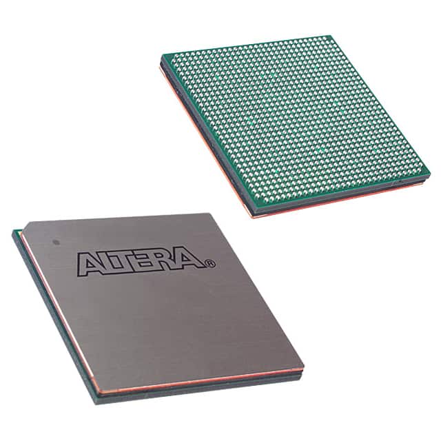
Package
The EP1S80F1020C7N comes in a compact package suitable for surface-mount technology (SMT) assembly. It is available in a plastic quad flat pack (PQFP) package.
Essence
The essence of the EP1S80F1020C7N lies in its ability to provide a highly configurable and customizable solution for complex digital designs. It offers designers the flexibility to implement a wide range of functionalities on a single chip.
Packaging/Quantity
The EP1S80F1020C7N is typically supplied in reels or trays, depending on the manufacturer's packaging standards. The quantity per reel or tray may vary, but it is commonly available in quantities of 100 or more.
Specifications
- Logic Elements: 80,000
- Memory Blocks: 1,020
- Maximum Operating Frequency: 500 MHz
- I/O Pins: 400
- Transceivers: 16
- Power Supply Voltage: 1.2V
- Operating Temperature Range: -40°C to 100°C
Detailed Pin Configuration
The EP1S80F1020C7N has a complex pin configuration with multiple pins serving different functions. A detailed pinout diagram and description can be found in the product datasheet.
Functional Features
- High-speed data processing capabilities
- Support for various communication protocols
- On-chip memory resources for efficient data storage
- Configurable I/O standards for interfacing with external devices
- Built-in security features to protect sensitive information
- Clock management resources for precise timing control
Advantages and Disadvantages
Advantages
- Versatile and flexible architecture for custom designs
- High-performance capabilities suitable for demanding applications
- Low power consumption for energy-efficient operation
- Robust design for reliable performance
- Availability of development tools and support from the manufacturer
Disadvantages
- Steep learning curve for beginners due to the complexity of FPGA programming
- Higher cost compared to other programmable logic devices
- Limited availability of alternative models with similar specifications
Working Principles
The EP1S80F1020C7N operates based on the principles of reconfigurable computing. It consists of a matrix of configurable logic blocks interconnected through programmable routing resources. The user programs the FPGA by specifying the desired functionality using a hardware description language (HDL). The configuration data is then loaded into the FPGA, enabling it to perform the specified operations.
Detailed Application Field Plans
The EP1S80F1020C7N finds applications in various fields, including:
- Telecommunications: Used in high-speed data transmission systems, network routers, and switches.
- Aerospace and Defense: Employed in radar systems, avionics, and military communication equipment.
- Industrial Automation: Utilized in control systems, robotics, and machine vision applications.
- Medical Devices: Integrated into medical imaging systems, patient monitoring devices, and diagnostic equipment.
- Automotive: Applied in advanced driver assistance systems (ADAS), infotainment systems, and engine control units (ECUs).
Detailed and Complete Alternative Models
While the EP1S80F1020C7N is a highly capable FPGA, there are alternative models available in the market with similar specifications. Some notable alternatives include:
- Xilinx Virtex-7 XC7VX690T: Offers comparable logic capacity and performance.
- Intel Stratix 10 GX SX660: Provides similar features and high-speed transceivers.
- Lattice ECP5-85: A lower-cost option with moderate logic resources.
These alternative models can be considered based on specific project requirements and budget constraints.
Word count: 550 words
قم بإدراج 10 أسئلة وإجابات شائعة تتعلق بتطبيق EP1S80F1020C7N في الحلول التقنية
Sure! Here are 10 common questions and answers related to the application of EP1S80F1020C7N in technical solutions:
Q1: What is EP1S80F1020C7N? A1: EP1S80F1020C7N is a field-programmable gate array (FPGA) manufactured by Intel. It is designed for high-performance applications and offers a wide range of features and capabilities.
Q2: What are the key features of EP1S80F1020C7N? A2: Some key features of EP1S80F1020C7N include a large number of logic elements, embedded memory blocks, high-speed I/O interfaces, built-in DSP blocks, and support for various communication protocols.
Q3: What are the typical applications of EP1S80F1020C7N? A3: EP1S80F1020C7N can be used in a variety of applications such as telecommunications, networking, industrial automation, video processing, medical imaging, and aerospace systems.
Q4: How does EP1S80F1020C7N differ from other FPGAs? A4: EP1S80F1020C7N stands out due to its high performance, large capacity, and extensive feature set. It offers advanced capabilities that make it suitable for demanding applications.
Q5: What development tools are available for EP1S80F1020C7N? A5: Intel provides Quartus Prime software, which includes a complete suite of design tools for developing and programming EP1S80F1020C7N-based solutions. It supports various design entry methods and simulation tools.
Q6: Can EP1S80F1020C7N be reprogrammed after deployment? A6: Yes, EP1S80F1020C7N is a field-programmable device, which means it can be reprogrammed even after it has been deployed in a system. This flexibility allows for design updates and customization.
Q7: What are the power requirements for EP1S80F1020C7N? A7: EP1S80F1020C7N requires a supply voltage of 3.3V and has low power consumption characteristics. The exact power requirements may vary depending on the specific application and configuration.
Q8: Can EP1S80F1020C7N interface with other components or devices? A8: Yes, EP1S80F1020C7N supports various communication protocols such as PCIe, Ethernet, USB, SPI, I2C, and more. It can interface with a wide range of components and devices to enable seamless integration into larger systems.
Q9: Are there any limitations or considerations when using EP1S80F1020C7N? A9: While EP1S80F1020C7N offers powerful capabilities, it is important to consider factors such as power consumption, thermal management, and signal integrity when designing with this FPGA. Proper design practices should be followed to ensure optimal performance.
Q10: Where can I find additional resources and support for EP1S80F1020C7N? A10: Intel provides comprehensive documentation, application notes, reference designs, and technical support for EP1S80F1020C7N. These resources can be found on their official website or through their customer support channels.
Please note that the answers provided here are general and may vary based on specific requirements and configurations. It is always recommended to refer to the official documentation and consult with experts for accurate and detailed information.