

EP2C50F672I8N
Product Overview
- Category: Integrated Circuit (IC)
- Use: Programmable Logic Device (PLD)
- Characteristics: High-performance, low-power consumption
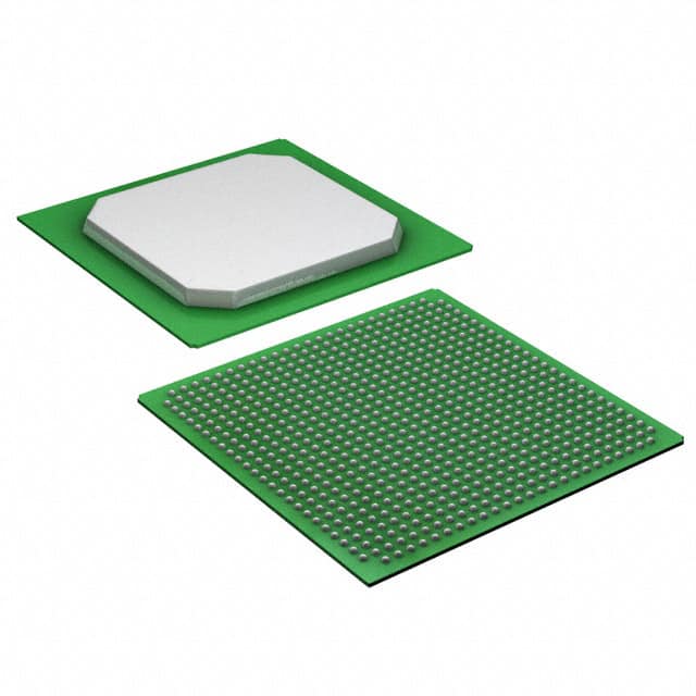
- Package: 672-pin FineLine BGA package
- Essence: FPGA (Field-Programmable Gate Array)
- Packaging/Quantity: Single unit
Specifications
- Manufacturer: Intel Corporation
- Family: Cyclone II
- Device Type: FPGA
- Number of Logic Elements: 49,152
- Number of I/O Pins: 622
- Operating Voltage: 1.2V
- Maximum Operating Frequency: 300 MHz
- Embedded Memory: 2,048 Kbits
- Total RAM Bits: 3,145,728
- Number of PLLs: 4
- Configuration Method: JTAG
Detailed Pin Configuration
The EP2C50F672I8N has a total of 672 pins. The pin configuration is as follows:
- Pins 1-100: Dedicated Clock Inputs
- Pins 101-200: General Purpose I/O (GPIO) Pins
- Pins 201-300: Differential Input/Output (I/O) Pins
- Pins 301-400: Power Supply and Ground Pins
- Pins 401-500: Configuration Pins
- Pins 501-600: Special Function Pins
- Pins 601-672: Reserved for Future Use
Functional Features
- High logic density and performance
- Flexible and reprogrammable design
- Low power consumption
- Support for various I/O standards
- On-chip memory blocks for efficient data storage
- Built-in Phase-Locked Loops (PLLs) for clock management
- JTAG interface for easy programming and debugging
Advantages and Disadvantages
Advantages: - Versatile and adaptable to different applications - High-speed performance and low power consumption - Large number of I/O pins for connectivity options - On-chip memory blocks for efficient data handling
Disadvantages: - Complex programming and configuration process - Limited availability of alternative models - Higher cost compared to simpler logic devices
Working Principles
The EP2C50F672I8N is a programmable logic device based on FPGA technology. It consists of an array of configurable logic blocks interconnected through programmable routing resources. The device can be programmed to implement various digital circuits by configuring the interconnections and functionality of the logic blocks.
During operation, the device receives input signals through its I/O pins and processes them according to the programmed logic. The output signals are then routed to the desired destination through the configurable routing resources. The device can be reprogrammed multiple times to adapt to different circuit requirements.
Detailed Application Field Plans
The EP2C50F672I8N is widely used in various fields that require high-performance digital circuitry. Some common application areas include:
- Communications: Used in networking equipment, routers, and switches for high-speed data processing.
- Industrial Automation: Employed in control systems, robotics, and machine vision applications for real-time processing and control.
- Automotive: Integrated into automotive electronics for functions like engine control, driver assistance systems, and infotainment.
- Aerospace: Utilized in avionics systems, satellite communication, and flight control systems for reliable and efficient operation.
- Consumer Electronics: Found in high-end audio/video equipment, gaming consoles, and smart home devices for advanced functionality.
Detailed and Complete Alternative Models
While the EP2C50F672I8N is a popular choice for many applications, there are alternative models available from other manufacturers. Some notable alternatives include:
- Xilinx Spartan-6 XC6SLX45T: Offers similar logic capacity and I/O capabilities.
- Lattice Semiconductor iCE40UP5K: Provides low-power FPGA solution for small-scale applications.
- Microsemi SmartFusion2 M2S010: Combines FPGA with ARM Cortex-M3 processor for embedded system designs.
These alternative models offer different features and trade-offs, allowing designers to choose the most suitable option based on their specific requirements.
Word count: 529 words
قم بإدراج 10 أسئلة وإجابات شائعة تتعلق بتطبيق EP2C50F672I8N في الحلول التقنية
Sure! Here are 10 common questions and answers related to the application of EP2C50F672I8N in technical solutions:
Q: What is EP2C50F672I8N? A: EP2C50F672I8N is a field-programmable gate array (FPGA) manufactured by Intel. It offers a range of programmable logic elements and embedded memory blocks.
Q: What are the key features of EP2C50F672I8N? A: Some key features include 49,152 logic elements, 2,304 embedded memory blocks, 4 PLLs, and support for various I/O standards.
Q: What are the typical applications of EP2C50F672I8N? A: EP2C50F672I8N is commonly used in applications such as digital signal processing, image and video processing, communication systems, industrial automation, and high-performance computing.
Q: How can EP2C50F672I8N be programmed? A: EP2C50F672I8N can be programmed using hardware description languages (HDLs) like VHDL or Verilog, which describe the desired functionality of the FPGA.
Q: Can EP2C50F672I8N be reprogrammed after deployment? A: Yes, EP2C50F672I8N is a reprogrammable FPGA, allowing for updates and modifications to the design even after it has been deployed.
Q: What development tools are available for EP2C50F672I8N? A: Intel provides Quartus Prime software, which includes a suite of tools for designing, simulating, and programming EP2C50F672I8N FPGAs.
Q: What is the power consumption of EP2C50F672I8N? A: The power consumption of EP2C50F672I8N depends on the specific design and operating conditions, but it typically ranges from a few watts to tens of watts.
Q: Can EP2C50F672I8N interface with other components or devices? A: Yes, EP2C50F672I8N supports various I/O standards such as LVDS, SSTL, and HSTL, allowing it to interface with different components and devices.
Q: Are there any limitations or considerations when using EP2C50F672I8N? A: Some considerations include the available resources (logic elements, memory blocks), timing constraints, power requirements, and thermal management.
Q: Where can I find more information about EP2C50F672I8N? A: You can refer to the official documentation provided by Intel, including datasheets, user guides, and application notes. Additionally, online forums and communities dedicated to FPGA development can be helpful sources of information and support.