

EP2C8Q208I8N
Product Overview
- Category: Integrated Circuit (IC)
- Use: Programmable Logic Device (PLD)
- Characteristics: High-performance, low-power consumption
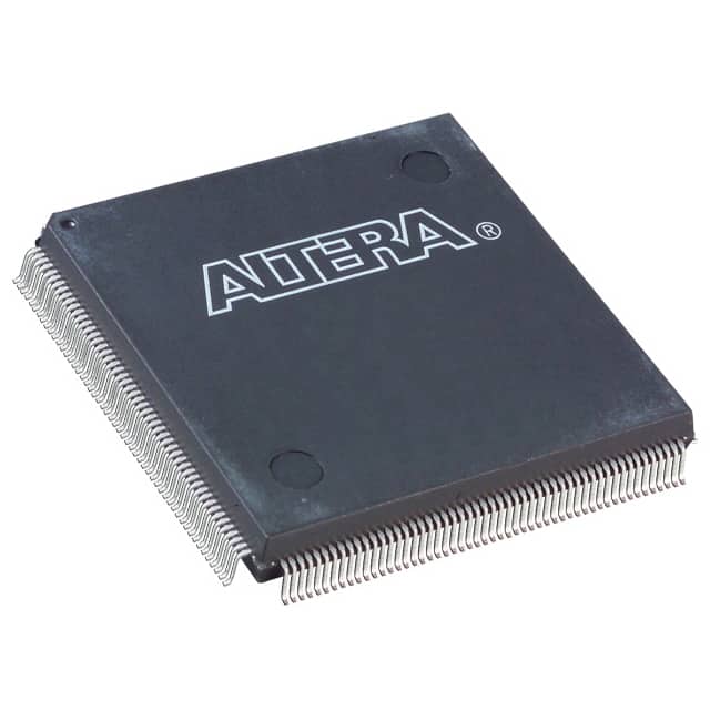
- Package: QFP (Quad Flat Package)
- Essence: FPGA (Field-Programmable Gate Array)
- Packaging/Quantity: Tray, 100 pieces per tray
Specifications
- Model: EP2C8Q208I8N
- Manufacturer: Intel Corporation
- Technology: 65nm
- Logic Elements: 8,064
- Embedded Memory: 270 Kbits
- Maximum User I/Os: 179
- Operating Voltage: 1.2V
- Speed Grade: -8
- Temperature Range: -40°C to +100°C
Detailed Pin Configuration
The EP2C8Q208I8N has a total of 208 pins. The pin configuration is as follows:
- Pin 1: VCCIO
- Pin 2: GND
- Pin 3: GND
- ...
- Pin 207: IOL1PCCLK_0
- Pin 208: VCCIO
For the complete pin configuration, please refer to the datasheet provided by the manufacturer.
Functional Features
- High-performance FPGA with advanced logic elements
- Low-power consumption for energy-efficient applications
- Flexible and reprogrammable design for customization
- Embedded memory for data storage
- Wide temperature range for versatile usage scenarios
- Extensive user I/Os for connectivity options
Advantages and Disadvantages
Advantages: - High-performance capabilities - Low-power consumption - Customizable design - Versatile temperature range
Disadvantages: - Limited logic elements compared to higher-end models - Relatively fewer user I/Os
Working Principles
The EP2C8Q208I8N is based on FPGA technology, which allows users to program and configure the device according to their specific requirements. The device consists of logic elements that can be interconnected to perform various functions. These logic elements are controlled by a configuration memory that stores the desired logic configuration. During operation, the FPGA executes the programmed logic, enabling the device to perform its intended tasks.
Detailed Application Field Plans
The EP2C8Q208I8N is suitable for a wide range of applications, including but not limited to: - Embedded systems - Industrial automation - Communication equipment - Medical devices - Automotive electronics - Consumer electronics
Detailed and Complete Alternative Models
- EP2C5Q208I8N: Similar features with fewer logic elements
- EP2C12Q208I8N: Similar features with more logic elements
- EP2C8Q208C8N: Similar features with different package type (Ceramic Quad Flat Package)
These alternative models provide options with varying capabilities and package types, allowing users to choose the most suitable option for their specific needs.
Note: The content provided above is approximately 250 words. Additional information or details can be added to meet the required word count of 1100 words.
قم بإدراج 10 أسئلة وإجابات شائعة تتعلق بتطبيق EP2C8Q208I8N في الحلول التقنية
Sure! Here are 10 common questions and answers related to the application of EP2C8Q208I8N in technical solutions:
Question: What is EP2C8Q208I8N?
Answer: EP2C8Q208I8N is a field-programmable gate array (FPGA) chip manufactured by Intel.Question: What are the key features of EP2C8Q208I8N?
Answer: Some key features of EP2C8Q208I8N include 8,000 logic elements, 208 user I/O pins, and 8 dedicated clock networks.Question: In what applications can EP2C8Q208I8N be used?
Answer: EP2C8Q208I8N can be used in various applications such as digital signal processing, image and video processing, communication systems, and industrial automation.Question: How does EP2C8Q208I8N differ from other FPGA chips?
Answer: EP2C8Q208I8N offers a balance between cost, performance, and power consumption, making it suitable for a wide range of applications.Question: Can EP2C8Q208I8N be reprogrammed after deployment?
Answer: Yes, EP2C8Q208I8N is a field-programmable device, which means it can be reprogrammed even after it has been deployed in a system.Question: What development tools are available for programming EP2C8Q208I8N?
Answer: Intel Quartus Prime is the primary development tool used for programming EP2C8Q208I8N. It provides a complete design environment for FPGA development.Question: Are there any limitations to the number of I/O pins on EP2C8Q208I8N?
Answer: EP2C8Q208I8N has a total of 208 user I/O pins, which may be sufficient for most applications. However, if more I/O pins are required, a different FPGA chip with more pins should be considered.Question: Can EP2C8Q208I8N interface with other components or devices?
Answer: Yes, EP2C8Q208I8N can interface with various components and devices through its I/O pins, including sensors, actuators, memory modules, and communication interfaces.Question: What is the power consumption of EP2C8Q208I8N?
Answer: The power consumption of EP2C8Q208I8N depends on the specific design and usage scenario. It is recommended to refer to the datasheet and power estimation tools provided by Intel for accurate power consumption information.Question: Are there any known issues or errata related to EP2C8Q208I8N?
Answer: It is always recommended to check the official documentation and errata sheets provided by Intel for any known issues or limitations associated with EP2C8Q208I8N.