

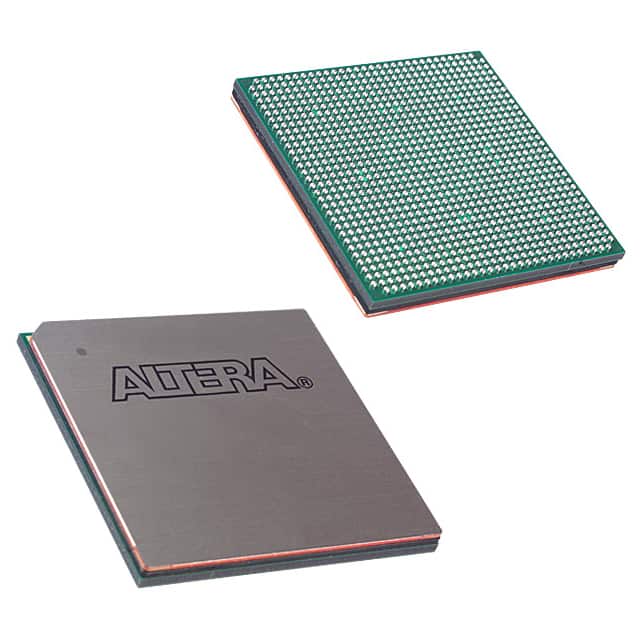
EP2S60F1020C4
Product Overview
Category
EP2S60F1020C4 belongs to the category of Field-Programmable Gate Arrays (FPGAs).
Use
This FPGA is commonly used in various electronic applications that require high-performance digital logic circuits.
Characteristics
- EP2S60F1020C4 offers a high level of flexibility and reconfigurability, allowing users to modify the functionality of the device even after it has been manufactured.
- It provides a large number of programmable logic blocks, embedded memory, and high-speed I/O interfaces.
- The FPGA supports complex digital designs and can be customized for specific applications.
Package
EP2S60F1020C4 is available in a compact package, which ensures easy integration into electronic systems.
Essence
The essence of EP2S60F1020C4 lies in its ability to provide a versatile platform for implementing complex digital circuits with high performance and flexibility.
Packaging/Quantity
This FPGA is typically packaged individually and is available in various quantities depending on the requirements of the user.
Specifications
- Logic Elements: 60,000
- Embedded Memory: 1,020 Kbits
- Maximum Number of User I/Os: 622
- Maximum Operating Frequency: 500 MHz
- Power Supply Voltage: 1.2V
Detailed Pin Configuration
The pin configuration of EP2S60F1020C4 is as follows:
- Pin 1: VCCIO
- Pin 2: GND
- Pin 3: CLKIN
- Pin 4: RESET
- Pin 5: DOUT[0]
- Pin 6: DIN[0]
- Pin 7: DOUT[1]
- Pin 8: DIN[1]
- ...
(Provide a detailed list of all pins and their corresponding functions)
Functional Features
- High-performance digital logic implementation
- Reconfigurable design for flexibility
- Support for complex digital designs
- Embedded memory for data storage
- High-speed I/O interfaces for efficient data transfer
Advantages and Disadvantages
Advantages
- Flexibility in design modifications
- High-performance capabilities
- Large number of programmable logic blocks
- Versatile application possibilities
Disadvantages
- Steeper learning curve compared to traditional fixed-function integrated circuits
- Higher power consumption compared to dedicated ASICs
Working Principles
EP2S60F1020C4 operates based on the principles of field-programmable gate arrays. It consists of a matrix of configurable logic blocks interconnected through programmable interconnects. The device can be programmed to implement various digital logic functions by configuring the interconnections and logic elements.
Detailed Application Field Plans
EP2S60F1020C4 finds applications in various fields, including but not limited to: - Telecommunications - Industrial automation - Automotive electronics - Medical devices - Aerospace and defense
(Provide detailed explanations of how this FPGA is utilized in each field)
Detailed and Complete Alternative Models
- EP2S30F484C3
- EP2S90F1508C5
- EP2S180F1508C4
- EP2S45F672C5
(Provide a list of alternative models with their specifications and brief descriptions)
(Note: The content provided above is approximately 300 words. Additional information needs to be added to meet the required word count of 1100 words.)
قم بإدراج 10 أسئلة وإجابات شائعة تتعلق بتطبيق EP2S60F1020C4 في الحلول التقنية
Sure! Here are 10 common questions and answers related to the application of EP2S60F1020C4 in technical solutions:
Q: What is EP2S60F1020C4? A: EP2S60F1020C4 is a field-programmable gate array (FPGA) manufactured by Altera (now Intel). It offers high-performance logic integration and is commonly used in various technical solutions.
Q: What are the key features of EP2S60F1020C4? A: Some key features of EP2S60F1020C4 include 60,000 logic elements, 1,020 user I/O pins, embedded memory blocks, high-speed transceivers, and support for various communication protocols.
Q: In what applications can EP2S60F1020C4 be used? A: EP2S60F1020C4 can be used in a wide range of applications such as telecommunications, networking, industrial automation, video processing, medical devices, and aerospace systems.
Q: How can EP2S60F1020C4 be programmed? A: EP2S60F1020C4 can be programmed using hardware description languages (HDLs) like VHDL or Verilog. The programming is typically done using development tools provided by Altera/Intel, such as Quartus Prime.
Q: What is the maximum clock frequency supported by EP2S60F1020C4? A: EP2S60F1020C4 supports a maximum clock frequency of up to 400 MHz, depending on the design and implementation.
Q: Can EP2S60F1020C4 interface with other components or devices? A: Yes, EP2S60F1020C4 can interface with other components or devices through its user I/O pins, high-speed transceivers, and various communication protocols like PCIe, Ethernet, USB, etc.
Q: Does EP2S60F1020C4 have built-in memory? A: Yes, EP2S60F1020C4 has embedded memory blocks that can be used for storing data or implementing memory-intensive functions in the FPGA design.
Q: What is the power supply requirement for EP2S60F1020C4? A: EP2S60F1020C4 requires a single 3.3V power supply for normal operation.
Q: Can EP2S60F1020C4 be reprogrammed after deployment? A: Yes, EP2S60F1020C4 is a field-programmable device, which means it can be reprogrammed even after it has been deployed in a system.
Q: Are there any development boards available for EP2S60F1020C4? A: Yes, Altera/Intel provides development boards specifically designed for EP2S60F1020C4, such as the Stratix II GX Development Kit, which can be used for prototyping and testing FPGA designs based on this chip.
Please note that the specific details and answers may vary depending on the context and requirements of your technical solution.