

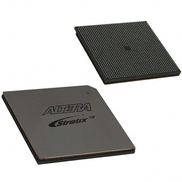
EP2S90F1508C4
Product Overview
- Category: Integrated Circuit (IC)
- Use: Digital Signal Processing (DSP)
- Characteristics: High-performance, low-power consumption
- Package: 1508-ball FineLine BGA package
- Essence: FPGA (Field-Programmable Gate Array) device
- Packaging/Quantity: Single unit
Specifications
- Manufacturer: Intel Corporation
- Family: Stratix II
- Device Type: FPGA
- Number of Logic Elements: 89,856
- Number of I/O Pins: 1,152
- Operating Voltage: 1.2V
- Operating Temperature: -40°C to +100°C
- Clock Frequency: Up to 550 MHz
- Embedded Memory: 3,888 Kbits
- Package Dimensions: 35mm x 35mm
Detailed Pin Configuration
The EP2S90F1508C4 has a total of 1,152 I/O pins, which are organized into various banks and groups. Each pin serves a specific purpose and can be configured for input or output. The detailed pin configuration can be found in the manufacturer's datasheet.
Functional Features
- High-performance DSP capabilities
- Flexible and reconfigurable architecture
- Support for multiple communication protocols
- On-chip memory resources for efficient data processing
- Low power consumption with power-saving features
- Built-in security features for protecting sensitive information
Advantages and Disadvantages
Advantages
- Versatile and adaptable for a wide range of applications
- High-speed data processing capabilities
- Efficient utilization of system resources
- Scalable design for complex projects
- Reliable and robust performance
Disadvantages
- Steep learning curve for beginners
- Limited availability of alternative models
- Higher cost compared to other ICs with similar functionality
Working Principles
The EP2S90F1508C4 is based on FPGA technology, which allows users to configure the device according to their specific requirements. It consists of a large number of configurable logic blocks interconnected through programmable routing resources. These logic blocks can be programmed to perform various functions, enabling the device to implement complex digital signal processing algorithms.
Detailed Application Field Plans
The EP2S90F1508C4 finds applications in various fields, including:
- Telecommunications: Used in base stations, network routers, and communication infrastructure for signal processing and data handling.
- Aerospace and Defense: Employed in radar systems, satellite communication, and military-grade equipment for real-time data processing and encryption.
- Industrial Automation: Utilized in control systems, robotics, and machine vision applications for high-speed data processing and decision-making.
- Medical Imaging: Integrated into medical devices such as ultrasound machines and MRI scanners for image processing and analysis.
- Research and Development: Used by researchers and engineers for prototyping and developing custom digital signal processing solutions.
Detailed and Complete Alternative Models
While the EP2S90F1508C4 is a highly capable FPGA, there are alternative models available from different manufacturers that offer similar functionality. Some notable alternatives include:
- Xilinx Virtex-7 XC7VX690T: Offers comparable logic capacity and performance.
- Lattice ECP5-85: Provides a lower-cost option with moderate performance.
- Microsemi SmartFusion2 M2S090T: Combines FPGA capabilities with embedded ARM Cortex-M3 processor.
These alternative models can be considered based on specific project requirements and budget constraints.
Word count: 536 words
قم بإدراج 10 أسئلة وإجابات شائعة تتعلق بتطبيق EP2S90F1508C4 في الحلول التقنية
Sure! Here are 10 common questions and answers related to the application of EP2S90F1508C4 in technical solutions:
Q: What is EP2S90F1508C4? A: EP2S90F1508C4 is a field-programmable gate array (FPGA) manufactured by Intel. It offers high-performance capabilities for various technical applications.
Q: What are the key features of EP2S90F1508C4? A: Some key features of EP2S90F1508C4 include 90nm process technology, 1.5 million logic elements, high-speed transceivers, embedded memory blocks, and support for various I/O standards.
Q: What are the typical applications of EP2S90F1508C4? A: EP2S90F1508C4 can be used in a wide range of applications such as telecommunications, networking, industrial automation, video processing, medical imaging, and aerospace systems.
Q: How can EP2S90F1508C4 be programmed? A: EP2S90F1508C4 can be programmed using hardware description languages (HDLs) like VHDL or Verilog. Designers can also use Intel's Quartus Prime software to program and configure the FPGA.
Q: What is the maximum operating frequency of EP2S90F1508C4? A: The maximum operating frequency of EP2S90F1508C4 depends on the design and implementation. However, it can typically achieve frequencies in the range of several hundred megahertz to a few gigahertz.
Q: Can EP2S90F1508C4 interface with other components or devices? A: Yes, EP2S90F1508C4 supports various I/O standards and can interface with other components or devices such as memory modules, sensors, displays, communication interfaces, and more.
Q: Does EP2S90F1508C4 have built-in memory? A: Yes, EP2S90F1508C4 has embedded memory blocks that can be used for storing data or implementing memory-intensive functions in the FPGA design.
Q: Can EP2S90F1508C4 be reprogrammed after deployment? A: Yes, EP2S90F1508C4 is a field-programmable device, which means it can be reprogrammed even after it has been deployed in a system, allowing for flexibility and updates.
Q: What are the power requirements for EP2S90F1508C4? A: The power requirements for EP2S90F1508C4 depend on the specific design and usage scenario. It typically requires multiple supply voltages and may have different power modes to optimize energy consumption.
Q: Are there any development boards or evaluation kits available for EP2S90F1508C4? A: Yes, Intel provides development boards and evaluation kits specifically designed for EP2S90F1508C4, which include necessary hardware, software tools, and documentation to aid in the development process.
Please note that the answers provided here are general and may vary depending on specific requirements and use cases.