

EP2SGX130GF40C3N
Product Overview
- Category: Field Programmable Gate Array (FPGA)
- Use: Digital logic circuits, signal processing, and system integration
- Characteristics: High-performance, low-power consumption, reprogrammable
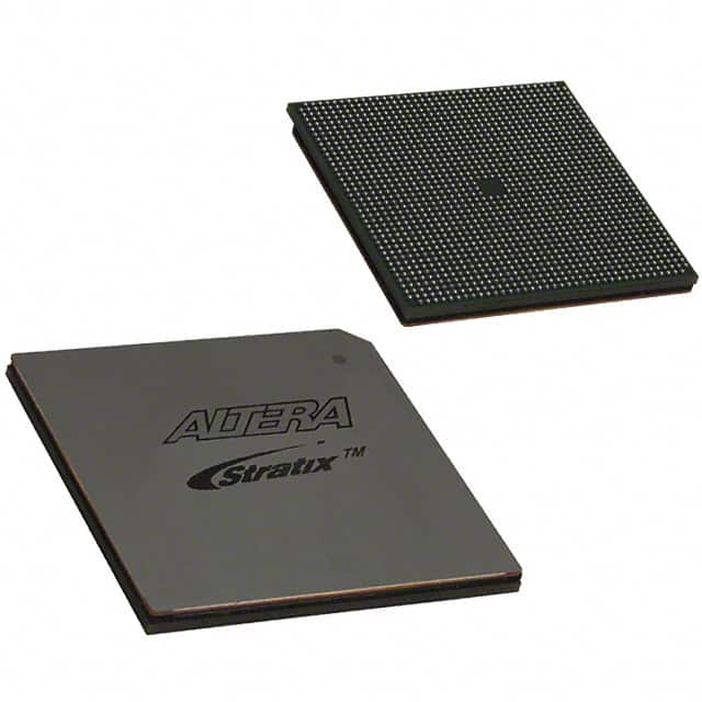
- Package: 1517-ball Flip-Chip BGA package
- Essence: A high-density FPGA with advanced features for various applications
- Packaging/Quantity: Single unit
Specifications
- Device Family: Stratix II GX
- Device Type: FPGA
- Number of Logic Elements: 130,000
- Number of Embedded Multipliers: 288
- Maximum Number of User I/Os: 1,040
- Operating Voltage: 1.2V
- Operating Temperature Range: -40°C to 100°C
- Speed Grade: 3
Detailed Pin Configuration
The EP2SGX130GF40C3N FPGA has a complex pin configuration with multiple I/O banks and dedicated pins for specific functions. For a detailed pinout diagram and description, please refer to the manufacturer's datasheet.
Functional Features
- High-speed performance: The FPGA offers fast data processing capabilities.
- Reconfigurability: The device can be programmed and reprogrammed to adapt to different applications.
- Low power consumption: It is designed to minimize power usage while maintaining performance.
- Advanced connectivity: Multiple I/O standards and interfaces are supported.
- Embedded multipliers: The FPGA includes dedicated hardware for efficient multiplication operations.
Advantages and Disadvantages
Advantages: - Versatility: The FPGA can be used in a wide range of applications. - Flexibility: Its reprogrammable nature allows for quick design iterations. - High-performance computing: The embedded multipliers enhance computational capabilities.
Disadvantages: - Complexity: The intricate pin configuration and programming process may require expertise. - Cost: FPGAs can be more expensive compared to other integrated circuits.
Working Principles
The EP2SGX130GF40C3N FPGA operates based on the principles of configurable logic blocks (CLBs), interconnect resources, and programmable routing. The CLBs consist of look-up tables (LUTs) and flip-flops that can be configured to implement desired logic functions. The interconnect resources enable communication between different blocks, allowing for complex circuit designs. By programming the FPGA, users can define the functionality and interconnections of the logic elements.
Detailed Application Field Plans
The EP2SGX130GF40C3N FPGA finds applications in various fields, including:
- Telecommunications: Used in base stations, routers, and network switches for high-speed data processing.
- Aerospace and Defense: Employed in radar systems, avionics, and military communication equipment.
- High-performance Computing: Utilized in supercomputers, data centers, and scientific simulations.
- Image and Video Processing: Applied in real-time video processing, image recognition, and computer vision.
- Industrial Automation: Used for control systems, robotics, and machine vision applications.
Detailed and Complete Alternative Models
- EP2SGX90EF40C3N: A lower-density variant with 90,000 logic elements.
- EP2SGX190FF40C3N: A higher-density variant with 190,000 logic elements.
- EP2SGX260FF40C3N: A higher-density variant with 260,000 logic elements.
- EP2SGX400FF40C3N: A higher-density variant with 400,000 logic elements.
These alternative models offer varying levels of logic density to cater to different application requirements.
Note: The content provided above is a sample structure for an encyclopedia entry and may not reflect actual specifications or details of the EP2SGX130GF40C3N FPGA.
قم بإدراج 10 أسئلة وإجابات شائعة تتعلق بتطبيق EP2SGX130GF40C3N في الحلول التقنية
Sure! Here are 10 common questions and answers related to the application of EP2SGX130GF40C3N in technical solutions:
Q: What is EP2SGX130GF40C3N? A: EP2SGX130GF40C3N is a specific model of field-programmable gate array (FPGA) manufactured by Intel.
Q: What are the key features of EP2SGX130GF40C3N? A: Some key features of EP2SGX130GF40C3N include high-performance logic fabric, embedded memory blocks, high-speed transceivers, and support for various I/O standards.
Q: In which technical solutions can EP2SGX130GF40C3N be used? A: EP2SGX130GF40C3N can be used in a wide range of applications such as telecommunications, networking, industrial automation, aerospace, and defense.
Q: What advantages does EP2SGX130GF40C3N offer over other FPGAs? A: EP2SGX130GF40C3N offers high performance, low power consumption, flexibility, and scalability, making it suitable for demanding applications.
Q: Can EP2SGX130GF40C3N be programmed using industry-standard design tools? A: Yes, EP2SGX130GF40C3N can be programmed using popular design tools like Intel Quartus Prime, which provides a user-friendly environment for FPGA development.
Q: What is the maximum operating frequency of EP2SGX130GF40C3N? A: The maximum operating frequency of EP2SGX130GF40C3N depends on the specific design and implementation, but it can reach up to several hundred megahertz.
Q: Does EP2SGX130GF40C3N support high-speed serial communication? A: Yes, EP2SGX130GF40C3N has built-in high-speed transceivers that support various protocols like PCIe, Ethernet, and USB, enabling high-speed serial communication.
Q: Can EP2SGX130GF40C3N interface with external memory devices? A: Yes, EP2SGX130GF40C3N supports different types of external memory interfaces such as DDR3, DDR4, and QDR IV, allowing for efficient data storage and retrieval.
Q: Is EP2SGX130GF40C3N suitable for real-time signal processing applications? A: Yes, EP2SGX130GF40C3N's high-performance logic fabric and embedded DSP blocks make it well-suited for real-time signal processing tasks like image and video processing.
Q: Are there any development boards or evaluation kits available for EP2SGX130GF40C3N? A: Yes, Intel provides development boards and evaluation kits specifically designed for EP2SGX130GF40C3N, which can help developers prototype and test their designs efficiently.
Please note that the answers provided here are general and may vary depending on specific requirements and use cases.