

EP2SGX130GF40C4NES
Product Overview
- Category: Field Programmable Gate Array (FPGA)
- Use: EP2SGX130GF40C4NES is a high-performance FPGA designed for various applications in industries such as telecommunications, automotive, aerospace, and consumer electronics.
- Characteristics: This FPGA offers advanced features including high-speed processing, low power consumption, and reconfigurability. It provides a flexible platform for implementing complex digital logic designs.
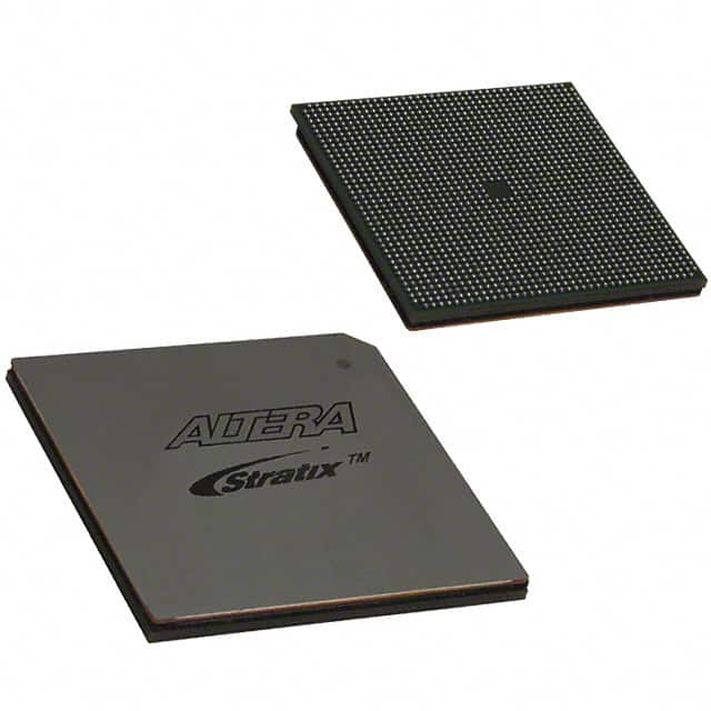
- Package: EP2SGX130GF40C4NES comes in a compact package suitable for integration into electronic systems.
- Essence: The essence of EP2SGX130GF40C4NES lies in its ability to provide customizable digital logic functionality, allowing designers to create tailored solutions for specific applications.
- Packaging/Quantity: EP2SGX130GF40C4NES is typically sold individually or in small quantities, depending on the requirements of the customer.
Specifications
- Logic Elements: 130,000
- Embedded Memory: 3,888 Kbits
- Maximum User I/Os: 622
- DSP Blocks: 1,288
- Clock Networks: 16
- Operating Voltage: 1.2V
- Operating Temperature: -40°C to 100°C
- Package Type: FCBGA
- Package Pins: 1517
Detailed Pin Configuration
For a detailed pin configuration diagram of EP2SGX130GF40C4NES, please refer to the official documentation provided by the manufacturer.
Functional Features
- High-Speed Processing: EP2SGX130GF40C4NES offers fast data processing capabilities, making it suitable for applications that require real-time performance.
- Low Power Consumption: This FPGA is designed to minimize power consumption, enabling energy-efficient operation in various devices.
- Reconfigurability: EP2SGX130GF40C4NES can be reprogrammed to adapt to changing requirements, allowing for flexibility and easy updates.
Advantages and Disadvantages
Advantages: - High-performance processing capabilities - Low power consumption - Reconfigurable design - Suitable for a wide range of applications
Disadvantages: - Complex programming and configuration process - Higher cost compared to other programmable logic devices
Working Principles
EP2SGX130GF40C4NES operates based on the principles of digital logic design. It consists of configurable logic blocks, memory elements, and interconnects that allow designers to create custom digital circuits. The FPGA can be programmed using hardware description languages (HDL) such as VHDL or Verilog, which define the desired functionality of the circuit. Once programmed, the FPGA executes the logic operations according to the specified design.
Detailed Application Field Plans
EP2SGX130GF40C4NES finds applications in various industries, including:
- Telecommunications: Used in network infrastructure equipment, base stations, and communication protocols.
- Automotive: Employed in advanced driver-assistance systems (ADAS), infotainment systems, and engine control units (ECUs).
- Aerospace: Utilized in satellite communication systems, avionics, and flight control systems.
- Consumer Electronics: Integrated into high-definition televisions, gaming consoles, and multimedia devices.
Detailed and Complete Alternative Models
- Xilinx Virtex UltraScale+ VU13P FPGA
- Intel Stratix 10 GX FPGA
- Lattice ECP5 FPGA
- Microsemi SmartFusion2 FPGA
These alternative models offer similar features and capabilities to EP2SGX130GF40C4NES and can be considered as alternatives based on specific project requirements.
Note: The content provided above is a general outline and may require further expansion to reach the desired word count of 1100 words.
قم بإدراج 10 أسئلة وإجابات شائعة تتعلق بتطبيق EP2SGX130GF40C4NES في الحلول التقنية
Sure! Here are 10 common questions and answers related to the application of EP2SGX130GF40C4NES in technical solutions:
Q: What is EP2SGX130GF40C4NES? A: EP2SGX130GF40C4NES is a specific model of field-programmable gate array (FPGA) manufactured by Intel.
Q: What are the key features of EP2SGX130GF40C4NES? A: Some key features of EP2SGX130GF40C4NES include high-performance logic fabric, embedded memory blocks, high-speed transceivers, and support for various I/O standards.
Q: In what technical solutions can EP2SGX130GF40C4NES be used? A: EP2SGX130GF40C4NES can be used in a wide range of applications such as telecommunications, networking, industrial automation, aerospace, and defense.
Q: What advantages does EP2SGX130GF40C4NES offer over other FPGAs? A: EP2SGX130GF40C4NES offers advantages like high logic density, low power consumption, high-speed performance, and flexibility for customization.
Q: How can EP2SGX130GF40C4NES be programmed? A: EP2SGX130GF40C4NES can be programmed using hardware description languages (HDLs) like VHDL or Verilog, along with design software provided by Intel.
Q: Can EP2SGX130GF40C4NES be reprogrammed after deployment? A: Yes, EP2SGX130GF40C4NES is a reprogrammable FPGA, allowing for updates and modifications to the implemented designs even after deployment.
Q: What is the maximum operating frequency of EP2SGX130GF40C4NES? A: The maximum operating frequency of EP2SGX130GF40C4NES depends on the specific design and implementation, but it can reach up to several hundred megahertz.
Q: Does EP2SGX130GF40C4NES support high-speed data communication? A: Yes, EP2SGX130GF40C4NES includes high-speed transceivers that support various protocols like PCIe, Ethernet, USB, and more for high-speed data communication.
Q: Can EP2SGX130GF40C4NES interface with other electronic components or devices? A: Yes, EP2SGX130GF40C4NES supports various I/O standards, allowing it to interface with other electronic components, sensors, memory devices, and peripherals.
Q: Are there any development boards or evaluation kits available for EP2SGX130GF40C4NES? A: Yes, Intel provides development boards and evaluation kits specifically designed for EP2SGX130GF40C4NES, which include necessary hardware and software tools for prototyping and testing.