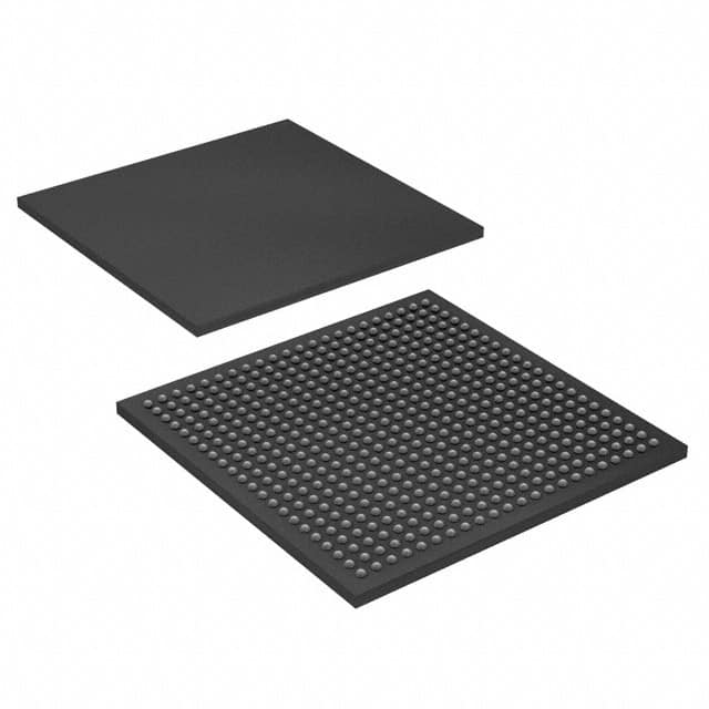
EPF10K100EFC484-3
Product Overview
Category: Programmable Logic Device (PLD)
Use: The EPF10K100EFC484-3 is a high-performance PLD designed for various digital logic applications. It offers flexible programmability and advanced features to meet the demands of complex designs.
Characteristics: - High-density integration - Low power consumption - Fast performance - Extensive I/O capabilities - Versatile design options
Package: The EPF10K100EFC484-3 comes in a 484-pin FineLine BGA package, which provides excellent thermal dissipation and compact form factor.
Essence: This PLD is built on a Field-Programmable Gate Array (FPGA) architecture, allowing users to configure its internal logic elements according to their specific requirements.
Packaging/Quantity: The EPF10K100EFC484-3 is typically sold individually in anti-static packaging to ensure safe handling during transportation and storage.
Specifications
- Logic Elements: 100,000
- Maximum User I/Os: 316
- Embedded Multiplier Blocks: 48
- Block RAM Bits: 1,152,000
- Clock Networks: 8
- Maximum Operating Frequency: 250 MHz
- Supply Voltage: 3.3V
- Operating Temperature Range: -40°C to +85°C
Pin Configuration
The EPF10K100EFC484-3 has a well-defined pinout configuration, which facilitates easy integration into various circuit designs. For detailed pin assignments, please refer to the manufacturer's datasheet.
Functional Features
Flexible Logic Configuration: The EPF10K100EFC484-3 allows users to program the internal logic elements using Hardware Description Languages (HDLs) or schematic entry tools, enabling the implementation of complex digital circuits.
Versatile I/O Capabilities: With 316 user I/Os, this PLD offers extensive connectivity options, allowing seamless integration with other components and peripherals.
High-Speed Performance: The device operates at a maximum frequency of 250 MHz, enabling rapid execution of logic operations and data processing.
Embedded Multiplier Blocks: The presence of 48 embedded multiplier blocks facilitates efficient multiplication and arithmetic calculations in digital designs.
Advantages
- High-density integration enables complex designs to be implemented on a single chip.
- Flexible programmability allows for iterative design changes without requiring physical modifications.
- Versatile I/O capabilities provide ample connectivity options for interfacing with external devices.
- Fast performance ensures quick execution of logic operations and data processing.
- Embedded multiplier blocks enhance computational efficiency in arithmetic-intensive applications.
Disadvantages
- Limited availability of user I/Os compared to larger PLDs may restrict the number of external connections in certain designs.
- Higher power consumption compared to low-power alternatives may not be suitable for battery-powered applications.
- Complexity of programming and configuring the PLD may require a learning curve for inexperienced users.
Working Principles
The EPF10K100EFC484-3 utilizes a reconfigurable FPGA architecture, which consists of an array of configurable logic elements interconnected through programmable routing resources. These logic elements can be programmed to implement various digital functions, such as combinatorial logic, sequential logic, and memory elements. The configuration data is stored in on-chip non-volatile memory, allowing the device to retain its programmed functionality even after power cycles.
Detailed Application Field Plans
The EPF10K100EFC484-3 finds applications in a wide range of fields, including but not limited to: - Telecommunications - Industrial automation - Automotive electronics - Aerospace and defense - Medical devices - Consumer electronics
Its versatility and high-performance characteristics make it suitable for applications that require complex digital logic processing, rapid data manipulation, and extensive connectivity.
Detailed and Complete Alternative Models
- EPF10K50SFC484-3: A lower-density variant of the EPF10K100EFC484-3, offering 50,000 logic elements and 208 user I/Os.
- EPF10K200SFC672-3: A higher-density variant with 200,000 logic elements and 424 user I/Os, providing increased capacity for larger designs.
- EPF10K30ATC144-3N: A compact PLD with 30,000 logic elements and 96 user I/Os, suitable for space-constrained applications.
These alternative models cater to different design requirements, allowing users to choose the most appropriate PLD based on their project specifications.
Word count: 570 words
قم بإدراج 10 أسئلة وإجابات شائعة تتعلق بتطبيق EPF10K100EFC484-3 في الحلول التقنية
Sure! Here are 10 common questions and answers related to the application of EPF10K100EFC484-3 in technical solutions:
Q: What is EPF10K100EFC484-3? A: EPF10K100EFC484-3 is a Field Programmable Gate Array (FPGA) manufactured by Intel (formerly Altera). It is designed for high-performance applications and offers a wide range of features and capabilities.
Q: What are the key features of EPF10K100EFC484-3? A: Some key features of EPF10K100EFC484-3 include 100,000 logic elements, 4-input look-up tables, embedded memory blocks, high-speed I/O interfaces, and support for various communication protocols.
Q: What are the typical applications of EPF10K100EFC484-3? A: EPF10K100EFC484-3 can be used in a variety of applications such as telecommunications, industrial automation, aerospace, defense systems, medical devices, and high-performance computing.
Q: How can EPF10K100EFC484-3 be programmed? A: EPF10K100EFC484-3 can be programmed using Hardware Description Languages (HDLs) like VHDL or Verilog. Design files are compiled using specialized software tools provided by Intel, which generate a configuration file that can be loaded onto the FPGA.
Q: Can EPF10K100EFC484-3 be reprogrammed multiple times? A: Yes, EPF10K100EFC484-3 is a reprogrammable FPGA, which means it can be reconfigured multiple times to implement different designs or functionality.
Q: What is the maximum operating frequency of EPF10K100EFC484-3? A: The maximum operating frequency of EPF10K100EFC484-3 depends on the design and implementation. It can typically operate at frequencies up to several hundred megahertz or even gigahertz.
Q: Does EPF10K100EFC484-3 support external memory interfaces? A: Yes, EPF10K100EFC484-3 supports various external memory interfaces such as DDR, SDRAM, SRAM, and Flash memory. These interfaces can be used to store and retrieve data during FPGA operation.
Q: Can EPF10K100EFC484-3 interface with other devices or peripherals? A: Yes, EPF10K100EFC484-3 provides a wide range of I/O interfaces including GPIOs, UARTs, SPI, I2C, Ethernet, and PCIe. These interfaces allow communication with external devices or peripherals.
Q: What are the power requirements for EPF10K100EFC484-3? A: EPF10K100EFC484-3 requires a supply voltage of 3.3V and has different power rails for core logic and I/O banks. The exact power requirements may vary depending on the specific design and configuration.
Q: Are there any development boards or evaluation kits available for EPF10K100EFC484-3? A: Yes, Intel provides development boards and evaluation kits specifically designed for EPF10K100EFC484-3. These kits include all the necessary hardware and software tools to get started with FPGA development.
Please note that the answers provided here are general and may vary based on specific requirements and implementations.


