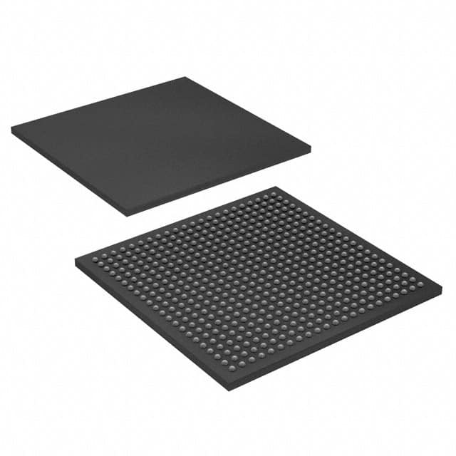
EPF10K30AFC484-2
Basic Information Overview
- Category: Programmable Logic Device (PLD)
- Use: EPF10K30AFC484-2 is a PLD used for digital logic applications.
- Characteristics:
- High-density programmable logic device
- Advanced CMOS technology
- Low power consumption
- Fast performance
- Package: The EPF10K30AFC484-2 comes in a 484-pin FineLine BGA package.
- Essence: EPF10K30AFC484-2 is designed to provide flexible and efficient digital logic implementation.
- Packaging/Quantity: The product is typically sold individually.
Specifications
- Logic Elements: 30,000
- Maximum User I/Os: 316
- Operating Voltage: 3.3V
- Speed Grade: -2 (indicating high-speed performance)
- Clock Management: Dedicated PLLs for clock generation and management
- Memory: Embedded memory blocks for data storage
- Configuration: In-system programmable via JTAG interface
Detailed Pin Configuration
The EPF10K30AFC484-2 has a total of 484 pins, each serving a specific purpose in the device's operation. A detailed pin configuration diagram can be found in the product datasheet.
Functional Features
- High-density programmable logic elements allow for complex digital circuit implementation.
- Dedicated PLLs enable precise clock generation and management.
- Embedded memory blocks provide on-chip data storage capabilities.
- In-system programmability allows for easy reconfiguration of the device.
Advantages
- High-density design enables the implementation of complex digital circuits.
- Low power consumption makes it suitable for power-sensitive applications.
- Fast performance ensures efficient execution of digital logic operations.
- In-system programmability allows for flexibility and ease of use.
Disadvantages
- Limited number of user I/Os may restrict the connectivity options in certain applications.
- FineLine BGA package may require specialized equipment for soldering and handling.
Working Principles
The EPF10K30AFC484-2 operates based on the principles of programmable logic. It consists of a large number of configurable logic elements that can be interconnected to implement desired digital logic functions. The device is programmed using a hardware description language (HDL) or a schematic entry tool, which configures the internal connections and functionality of the PLD.
Detailed Application Field Plans
The EPF10K30AFC484-2 finds applications in various fields where digital logic implementation is required. Some common application areas include: - Telecommunications - Industrial automation - Consumer electronics - Automotive electronics - Medical devices
Detailed and Complete Alternative Models
- EPF10K50SFC256-3: A higher-density version with 50,000 logic elements and 256-pin package.
- EPF10K100ABC356-1: A larger capacity PLD with 100,000 logic elements and 356-pin package.
- EPF10K200SBC600-2: An even higher-density model with 200,000 logic elements and 600-pin package.
These alternative models offer increased capacity and pin count, catering to different design requirements.
Word count: 345 words
قم بإدراج 10 أسئلة وإجابات شائعة تتعلق بتطبيق EPF10K30AFC484-2 في الحلول التقنية
Sure! Here are 10 common questions and answers related to the application of EPF10K30AFC484-2 in technical solutions:
Q: What is EPF10K30AFC484-2? A: EPF10K30AFC484-2 is a Field Programmable Gate Array (FPGA) manufactured by Intel (formerly Altera). It is designed for use in various electronic applications.
Q: What are the key features of EPF10K30AFC484-2? A: Some key features of EPF10K30AFC484-2 include 30,000 logic elements, 484-pin FineLine BGA package, embedded memory blocks, and support for various I/O standards.
Q: What are the typical applications of EPF10K30AFC484-2? A: EPF10K30AFC484-2 can be used in a wide range of applications such as telecommunications, industrial automation, medical devices, automotive systems, and aerospace.
Q: How can EPF10K30AFC484-2 be programmed? A: EPF10K30AFC484-2 can be programmed using hardware description languages (HDLs) like VHDL or Verilog, which are then synthesized into a configuration bitstream using design software.
Q: Can EPF10K30AFC484-2 be reprogrammed after initial programming? A: Yes, EPF10K30AFC484-2 is a reprogrammable FPGA, allowing for multiple iterations of designs and updates without the need for physical changes to the hardware.
Q: What are the power requirements for EPF10K30AFC484-2? A: EPF10K30AFC484-2 typically operates at a voltage range of 3.3V, with additional power supply requirements for I/O banks and other peripherals.
Q: Does EPF10K30AFC484-2 support different communication protocols? A: Yes, EPF10K30AFC484-2 supports various communication protocols such as UART, SPI, I2C, Ethernet, and CAN, which can be implemented using the available I/O pins.
Q: Can EPF10K30AFC484-2 interface with external memory devices? A: Yes, EPF10K30AFC484-2 has embedded memory blocks and can also interface with external memory devices like DDR SDRAM, SRAM, Flash memory, or EEPROM.
Q: What development tools are available for programming EPF10K30AFC484-2? A: Intel provides Quartus Prime software suite, which includes design entry, synthesis, simulation, and programming tools specifically tailored for programming FPGAs like EPF10K30AFC484-2.
Q: Are there any application-specific reference designs available for EPF10K30AFC484-2? A: Yes, Intel provides a wide range of reference designs and application notes that can help developers get started with EPF10K30AFC484-2 in specific applications, including motor control, image processing, and more.
Please note that the answers provided here are general and may vary depending on specific requirements and implementation details.


