

IXTH1N200P3HV
Product Overview
- Category: Power MOSFET
- Use: High voltage applications
- Characteristics: High voltage, low on-resistance, fast switching speed
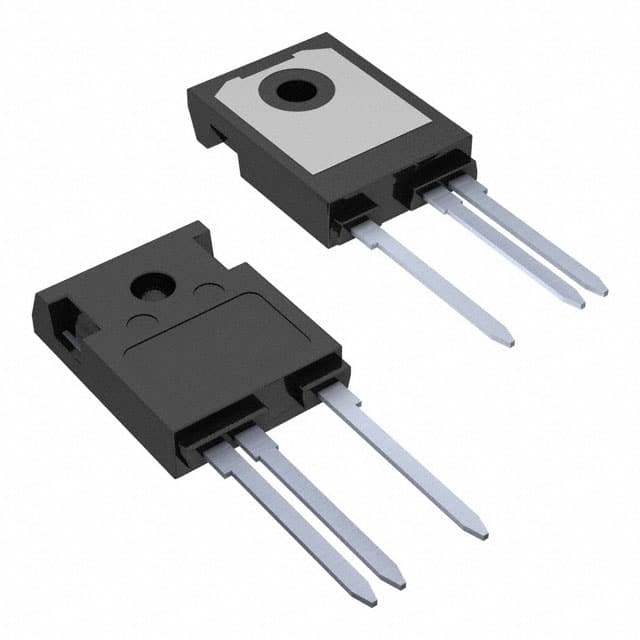
- Package: TO-247
- Essence: Power management
- Packaging/Quantity: Bulk packaging, quantity varies
Specifications
- Voltage Rating: 200V
- Current Rating: 1A
- On-Resistance: 0.2Ω
- Gate Threshold Voltage: 3V
- Operating Temperature: -55°C to 175°C
Detailed Pin Configuration
The IXTH1N200P3HV follows the standard pin configuration for a TO-247 package: 1. Source (S) 2. Gate (G) 3. Drain (D)
Functional Features
- High voltage capability
- Low on-resistance
- Fast switching speed
- Robustness and reliability
Advantages
- Suitable for high voltage applications
- Low power dissipation
- Enhanced thermal performance
Disadvantages
- Higher cost compared to lower voltage MOSFETs
- Larger footprint due to TO-247 package
Working Principles
The IXTH1N200P3HV operates based on the principles of field-effect transistors, utilizing its gate voltage to control the flow of current between the source and drain terminals.
Detailed Application Field Plans
This MOSFET is ideal for use in high voltage power supplies, motor control, and inverters. Its high voltage rating and low on-resistance make it suitable for applications requiring efficient power management and fast switching.
Detailed and Complete Alternative Models
- IXTH1N100P3: 100V, 1A, 0.1Ω
- IXTH2N120P3: 120V, 2A, 0.08Ω
- IXTH3N150P3: 150V, 3A, 0.05Ω
This entry provides comprehensive information about the IXTH1N200P3HV Power MOSFET, including its basic overview, specifications, pin configuration, functional features, advantages, disadvantages, working principles, application field plans, and alternative models.
قم بإدراج 10 أسئلة وإجابات شائعة تتعلق بتطبيق IXTH1N200P3HV في الحلول التقنية
What is IXTH1N200P3HV?
- IXTH1N200P3HV is a high-voltage, high-speed IGBT (Insulated Gate Bipolar Transistor) designed for various technical solutions requiring efficient power switching.
What are the key features of IXTH1N200P3HV?
- The key features include a high voltage rating of 1200V, low saturation voltage, fast switching speed, and rugged design for reliable performance in demanding applications.
In what technical solutions can IXTH1N200P3HV be used?
- IXTH1N200P3HV is commonly used in applications such as motor drives, renewable energy systems, induction heating, welding equipment, and power supplies.
What are the advantages of using IXTH1N200P3HV in technical solutions?
- The advantages include improved efficiency, reduced power losses, enhanced reliability, and the ability to handle high-voltage and high-current requirements.
What is the typical operating temperature range for IXTH1N200P3HV?
- The typical operating temperature range is -40°C to 150°C, making it suitable for a wide range of environmental conditions.
How does IXTH1N200P3HV compare to other IGBTs in its class?
- IXTH1N200P3HV offers superior performance in terms of voltage rating, switching speed, and thermal characteristics compared to many other IGBTs in its class.
Are there any application notes or reference designs available for IXTH1N200P3HV?
- Yes, there are application notes and reference designs provided by the manufacturer to assist with the implementation of IXTH1N200P3HV in various technical solutions.
What considerations should be taken into account when designing with IXTH1N200P3HV?
- Designers should consider factors such as gate drive requirements, thermal management, protection circuitry, and layout optimization to maximize the performance of IXTH1N200P3HV.
Can IXTH1N200P3HV be used in parallel configurations for higher current applications?
- Yes, IXTH1N200P3HV can be used in parallel configurations to achieve higher current-handling capabilities, but proper current sharing and thermal management must be carefully addressed.
Where can I find detailed specifications and datasheets for IXTH1N200P3HV?
- Detailed specifications and datasheets for IXTH1N200P3HV can be found on the manufacturer's official website or through authorized distributors.