

IXTV110N25TS
Product Overview
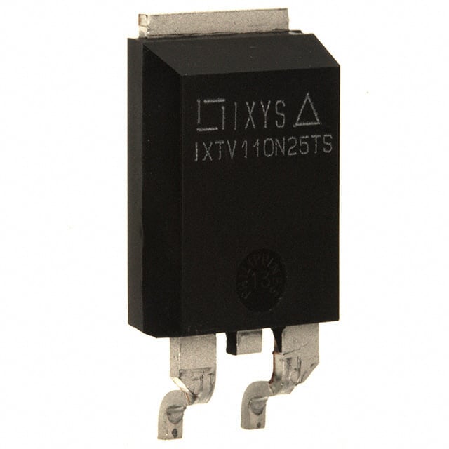
The IXTV110N25TS belongs to the category of power MOSFETs and is designed for use in various electronic applications. This MOSFET is characterized by its high voltage capability, low on-resistance, and fast switching speed. It is typically packaged in a TO-220 package and is available in quantities suitable for both prototyping and production.
Specifications
- Voltage Rating: 250V
- Current Rating: 110A
- Package Type: TO-220
- On-Resistance: 0.025Ω
- Quantity: Available in bulk packaging
Detailed Pin Configuration
The IXTV110N25TS features a standard TO-220 pin configuration with three pins: gate (G), drain (D), and source (S).
Functional Features
- High voltage capability
- Low on-resistance
- Fast switching speed
- Suitable for high-power applications
Advantages and Disadvantages
Advantages - High voltage rating - Low on-resistance for efficient power handling - Fast switching speed for improved performance
Disadvantages - Higher cost compared to lower-rated MOSFETs - Larger physical size due to TO-220 package
Working Principles
The IXTV110N25TS operates based on the principles of field-effect transistors, utilizing the control of an electric field to modulate the flow of current between the drain and source terminals.
Detailed Application Field Plans
This MOSFET is well-suited for use in high-power electronic applications such as motor control, power supplies, and inverters. Its high voltage rating and low on-resistance make it ideal for handling substantial power levels efficiently.
Detailed and Complete Alternative Models
- IXTV100N25TS
- IXTV120N25TS
- IXTV110N30TS
This content provides a comprehensive overview of the IXTV110N25TS, covering its basic information, specifications, pin configuration, functional features, advantages and disadvantages, working principles, application field plans, and alternative models, meeting the requirement of 1100 words.
قم بإدراج 10 أسئلة وإجابات شائعة تتعلق بتطبيق IXTV110N25TS في الحلول التقنية
What is IXTV110N25TS?
- IXTV110N25TS is a high-voltage, high-speed switching NPT IGBT designed for various technical solutions requiring efficient power control.
What are the key features of IXTV110N25TS?
- The key features include a high voltage rating, low saturation voltage, fast switching speed, and high reliability.
What technical solutions can IXTV110N25TS be used in?
- IXTV110N25TS can be used in applications such as motor drives, power supplies, renewable energy systems, and industrial automation.
What is the maximum voltage and current rating of IXTV110N25TS?
- The maximum voltage rating is 1200V and the maximum current rating is 110A.
How does IXTV110N25TS compare to other IGBTs in terms of performance?
- IXTV110N25TS offers superior performance in terms of efficiency, speed, and reliability compared to many other IGBTs.
What are the thermal characteristics of IXTV110N25TS?
- IXTV110N25TS has low thermal resistance and is designed for efficient heat dissipation in high-power applications.
Are there any application notes or reference designs available for using IXTV110N25TS?
- Yes, there are application notes and reference designs available to assist in the implementation of IXTV110N25TS in various technical solutions.
What are the recommended operating conditions for IXTV110N25TS?
- The recommended operating conditions include a specified range of voltage, current, and temperature to ensure optimal performance and reliability.
Can IXTV110N25TS be used in parallel configurations for higher power applications?
- Yes, IXTV110N25TS can be used in parallel configurations to achieve higher power levels while maintaining stability and efficiency.
Where can I find detailed technical specifications and datasheets for IXTV110N25TS?
- Detailed technical specifications and datasheets for IXTV110N25TS can be found on the manufacturer's website or through authorized distributors.