

LC4064ZC-37M56C
Product Overview
Category: Integrated Circuit (IC)
Use: The LC4064ZC-37M56C is a programmable logic device (PLD) that belongs to the family of Complex Programmable Logic Devices (CPLDs). It is designed for digital logic applications and offers high-performance, low-power consumption, and flexibility in circuit design.
Characteristics: - High-performance CPLD with 64 macrocells - Low power consumption - Flexible and reprogrammable logic functions - Wide operating voltage range - Small form factor
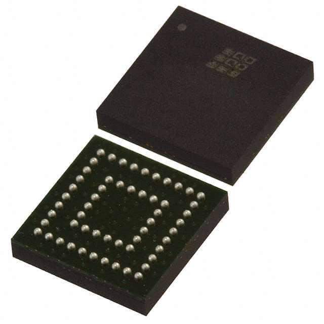
Package: The LC4064ZC-37M56C is available in a compact surface-mount package, which ensures easy integration into various electronic systems. The package type is typically indicated as "LC" or "LCC."
Essence: The essence of the LC4064ZC-37M56C lies in its ability to provide designers with a versatile and efficient solution for implementing complex digital logic circuits. Its programmability allows for customization and adaptation to specific application requirements.
Packaging/Quantity: The LC4064ZC-37M56C is commonly sold in reels or tubes, depending on the manufacturer's packaging standards. The quantity per package may vary, but it is typically supplied in multiples of 100 or 1000 units.
Specifications
The LC4064ZC-37M56C has the following specifications:
- Number of Macrocells: 64
- Operating Voltage Range: 3.0V - 5.5V
- Speed Grade: 37MHz
- Package Type: LCC
- Temperature Range: -40°C to +85°C
- I/O Pins: 56
- JTAG Boundary Scan Support: Yes
Detailed Pin Configuration
The LC4064ZC-37M56C has a total of 56 I/O pins, which are used for input and output connections. The pin configuration is as follows:
(Pin Number) - (Pin Name) 1 - VCCIO 2 - GND 3 - IO0 4 - IO1 5 - IO2 ... 56 - IO55
Functional Features
The LC4064ZC-37M56C offers the following functional features:
- Programmable logic functions: The device allows users to define custom logic functions using a Hardware Description Language (HDL) or a schematic editor.
- Macrocell architecture: The 64 macrocells can be individually programmed to perform specific logic operations, enabling complex circuit designs.
- Clock management: The device supports clock signals for synchronous operation, allowing precise timing control in digital systems.
- JTAG boundary scan: The built-in JTAG support facilitates testing and debugging of the device during development and production stages.
Advantages and Disadvantages
Advantages: - Versatility: The LC4064ZC-37M56C provides flexibility in designing complex digital logic circuits, making it suitable for a wide range of applications. - Low power consumption: The device is designed to minimize power consumption, making it ideal for battery-powered devices or energy-efficient systems. - Small form factor: The compact package size enables space-saving integration into electronic systems with limited board space.
Disadvantages: - Limited macrocell count: With only 64 macrocells, the LC4064ZC-37M56C may not be suitable for extremely large-scale logic designs that require a higher number of programmable elements. - Speed limitations: The speed grade of 37MHz may not be sufficient for applications that demand high-speed data processing or real-time operations.
Working Principles
The LC4064ZC-37M56C operates based on the principles of programmable logic. It consists of a matrix of configurable logic blocks (CLBs) and interconnect resources. The CLBs contain look-up tables (LUTs), flip-flops, and other elements that can be programmed to implement desired logic functions. The interconnect resources allow for the routing of signals between different CLBs.
During operation, the device is programmed using a hardware description language or a schematic editor. The user defines the desired logic functions and connections, which are then translated into configuration data. This data is loaded into the device, configuring the CLBs and interconnect resources accordingly. Once programmed, the LC4064ZC-37M56C performs the specified logic operations based on the input signals received.
Detailed Application Field Plans
The LC4064ZC-37M56C finds applications in various fields, including:
- Industrial Automation: The device can be used in control systems, monitoring equipment, and data acquisition systems.
- Communication Systems: It can be employed in network routers, switches, and communication interfaces.
- Consumer Electronics: The LC4064ZC-37M56C can be utilized in smart
قم بإدراج 10 أسئلة وإجابات شائعة تتعلق بتطبيق LC4064ZC-37M56C في الحلول التقنية
Sure! Here are 10 common questions and answers related to the application of LC4064ZC-37M56C in technical solutions:
1. What is LC4064ZC-37M56C? - LC4064ZC-37M56C is a specific model of Field Programmable Gate Array (FPGA) manufactured by Lattice Semiconductor.
2. What are the key features of LC4064ZC-37M56C? - The key features of LC4064ZC-37M56C include 64 macrocells, 64 I/O pins, 37 MHz maximum operating frequency, and 56-pin package.
3. What are the typical applications of LC4064ZC-37M56C? - LC4064ZC-37M56C is commonly used in various technical solutions such as industrial automation, telecommunications, automotive electronics, consumer electronics, and more.
4. How can LC4064ZC-37M56C be programmed? - LC4064ZC-37M56C can be programmed using Hardware Description Languages (HDLs) like VHDL or Verilog, which describe the desired functionality of the FPGA.
5. Can LC4064ZC-37M56C be reprogrammed after initial programming? - Yes, LC4064ZC-37M56C is a reprogrammable FPGA, allowing for multiple iterations and updates of the design.
6. What tools are available for programming LC4064ZC-37M56C? - Lattice Semiconductor provides software tools like Lattice Diamond or iCEcube2 that can be used for designing, simulating, and programming LC4064ZC-37M56C.
7. What voltage levels does LC4064ZC-37M56C support? - LC4064ZC-37M56C supports both 3.3V and 5V voltage levels, making it compatible with a wide range of systems.
8. Can LC4064ZC-37M56C interface with other components or devices? - Yes, LC4064ZC-37M56C can interface with various components and devices through its I/O pins, allowing for communication and integration within a larger system.
9. What is the power consumption of LC4064ZC-37M56C? - The power consumption of LC4064ZC-37M56C depends on the specific design and usage scenario. It is recommended to refer to the datasheet or use Lattice's power estimation tools for accurate power calculations.
10. Are there any application notes or reference designs available for LC4064ZC-37M56C? - Yes, Lattice Semiconductor provides application notes, reference designs, and technical documentation on their website, which can be helpful in understanding and implementing LC4064ZC-37M56C in various technical solutions.
Please note that the answers provided here are general and may vary depending on the specific requirements and context of the technical solution.