

LC4128V-75TN128C
Product Overview
Category: Integrated Circuit (IC)
Use: LC4128V-75TN128C is a programmable logic device (PLD) used for digital circuit design and implementation. It offers high-speed performance and flexibility, making it suitable for various applications.
Characteristics: - High-density programmable logic device - Low power consumption - Fast propagation delay - Flexible pin configuration - Wide operating temperature range
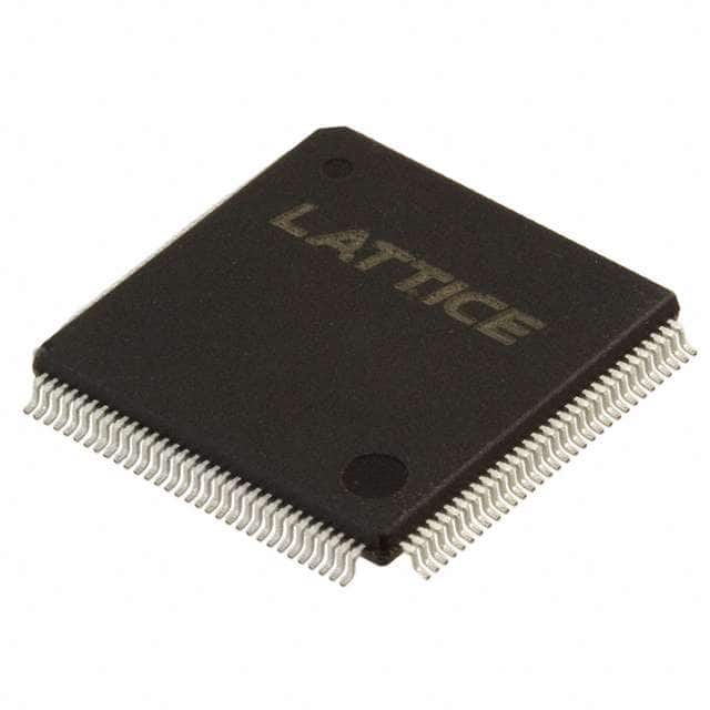
Package: LC4128V-75TN128C is available in a compact 128-pin Thin Quad Flat Pack (TQFP) package, which ensures easy integration into circuit boards.
Essence: The essence of LC4128V-75TN128C lies in its ability to provide reconfigurable logic functions, allowing designers to implement complex digital circuits efficiently.
Packaging/Quantity: Each package contains one LC4128V-75TN128C IC.
Specifications
- Logic Cells: 128
- Maximum Operating Frequency: 75 MHz
- Operating Voltage: 3.3V
- I/O Pins: 96
- Programmable Macrocells: 128
- On-Chip Memory: 2,048 bits
- JTAG Boundary Scan Support: Yes
Pin Configuration
The detailed pin configuration of LC4128V-75TN128C can be found in the datasheet provided by the manufacturer. It includes information about power supply pins, input/output pins, clock pins, and other control pins.
Functional Features
- High-Speed Performance: LC4128V-75TN128C offers fast propagation delay, enabling efficient execution of complex digital operations.
- Flexible Logic Design: With 128 programmable macrocells, designers have the freedom to implement a wide range of logic functions.
- Low Power Consumption: The IC is designed to minimize power consumption, making it suitable for battery-powered applications.
- JTAG Boundary Scan Support: The built-in JTAG boundary scan feature allows for easy testing and debugging of the device.
Advantages and Disadvantages
Advantages: - High-density programmable logic device - Fast propagation delay - Flexible pin configuration - Low power consumption - JTAG boundary scan support
Disadvantages: - Limited on-chip memory (2,048 bits) - Relatively high cost compared to simpler logic devices
Working Principles
LC4128V-75TN128C utilizes a combination of look-up tables (LUTs), flip-flops, and interconnect resources to implement digital logic functions. The device can be programmed using hardware description languages (HDL) or schematic entry tools, allowing designers to define the desired functionality.
During operation, the inputs are processed through the LUTs, which contain pre-defined truth tables. The output of the LUTs is then fed into the flip-flops, which store the state of the circuit. The interconnect resources provide the necessary connections between different logic elements.
Detailed Application Field Plans
LC4128V-75TN128C finds applications in various fields, including: 1. Embedded Systems: It can be used in microcontroller-based systems to implement custom peripheral interfaces or complex control logic. 2. Communications: LC4128V-75TN128C can be utilized in networking equipment for protocol handling, packet processing, and data manipulation. 3. Industrial Automation: It enables the implementation of control systems, motor control, and sensor interfacing in industrial automation applications. 4. Consumer Electronics: The IC can be employed in consumer electronics devices such as gaming consoles, set-top boxes, and audio/video equipment for custom logic implementation.
Alternative Models
- LC4128V-75TN128I: Similar to LC4128V-75TN128C but with industrial temperature range support.
- LC4128V-75TN128M: A higher-density version of the same IC, offering 256 logic cells.
- LC4032V-75TN128C: A lower-density alternative with 32 logic cells.
These alternative models provide options for different project requirements and budget considerations.
Word count: 511 words
قم بإدراج 10 أسئلة وإجابات شائعة تتعلق بتطبيق LC4128V-75TN128C في الحلول التقنية
Sure! Here are 10 common questions and answers related to the application of LC4128V-75TN128C in technical solutions:
Question: What is LC4128V-75TN128C?
Answer: LC4128V-75TN128C is a specific model of a low-power, high-density programmable logic device (PLD) manufactured by Lattice Semiconductor.Question: What are the key features of LC4128V-75TN128C?
Answer: Some key features of LC4128V-75TN128C include low power consumption, high density, 128 macrocells, and 75ns maximum propagation delay.Question: In what applications can LC4128V-75TN128C be used?
Answer: LC4128V-75TN128C can be used in various applications such as industrial control systems, automotive electronics, telecommunications, consumer electronics, and more.Question: How does LC4128V-75TN128C help in reducing power consumption?
Answer: LC4128V-75TN128C utilizes low-power CMOS technology and offers power-saving features like clock gating and dynamic power management, which help in reducing overall power consumption.Question: Can LC4128V-75TN128C be reprogrammed after deployment?
Answer: Yes, LC4128V-75TN128C is a programmable logic device, which means it can be reprogrammed multiple times even after it has been deployed in a system.Question: What development tools are available for programming LC4128V-75TN128C?
Answer: Lattice Semiconductor provides software tools like Lattice Diamond or ispLEVER Classic for designing, simulating, and programming LC4128V-75TN128C.Question: What is the maximum number of inputs and outputs supported by LC4128V-75TN128C?
Answer: LC4128V-75TN128C supports up to 128 inputs and outputs, which can be used for various digital signal processing tasks.Question: Can LC4128V-75TN128C interface with other components or devices?
Answer: Yes, LC4128V-75TN128C can interface with other components or devices using standard protocols like SPI, I2C, UART, or GPIO pins.Question: Are there any limitations or constraints when using LC4128V-75TN128C?
Answer: LC4128V-75TN128C has a limited number of macrocells and resources, so it may not be suitable for complex designs requiring a large number of logic elements.Question: Where can I find more information about LC4128V-75TN128C and its application in technical solutions?
Answer: You can refer to the datasheet and technical documentation provided by Lattice Semiconductor or consult their support team for more detailed information on LC4128V-75TN128C and its application in specific technical solutions.